Memory and its column decoding circuit

A memory and column decoding technology, which is applied in the field of memory and its column decoding circuit, can solve the problems of large memory power loss, etc., and achieve the effects of reducing power loss, reducing power loss, and reducing the amount of charge

Active Publication Date: 2017-02-08
SHANGHAI HUAHONG GRACE SEMICON MFG CORP
View PDF7 Cites 1 Cited by
  • Summary
  • Abstract
  • Description
  • Claims
  • Application Information

AI Technical Summary

Problems solved by technology

[0012] The present invention solves the problem of large memory power loss when using the existing memory row decoding circuit for read operation

Method used


Image

  • Memory and its column decoding circuit
  • Memory and its column decoding circuit
  • Memory and its column decoding circuit

Examples


Embodiment 1

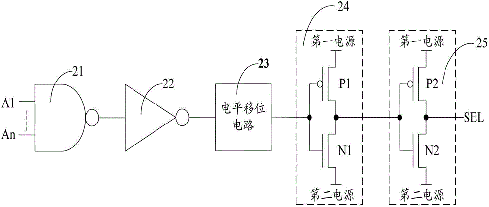
[0044] Figure 4 It is a structural schematic diagram of the column decoding circuit of the memory according to Embodiment 1 of the present invention. refer to Figure 4 The column decoding circuit of the memory includes a NAND gate circuit 41 , a NOT gate circuit 42 , a level shift circuit 43 and a first drive circuit 44 connected in sequence, and also includes a second drive circuit 45 and a precharge circuit 46 .

[0045] The second driving circuit 45 includes a first PMOS transistor P1, a first NMOS transistor N1 and a second NMOS transistor N2. The source of the first PMOS transistor P1 is adapted to be connected to a first power supply, the gate of the first PMOS transistor P1 is connected to the gate of the first NMOS transistor N1, and the drain of the first PMOS transistor P1 is connected to The drain of the first NMOS transistor N1, the source of the first NMOS transistor N1 is connected to the drain of the second NMOS transistor N2, and the gate of the second NMOS...

Embodiment 2

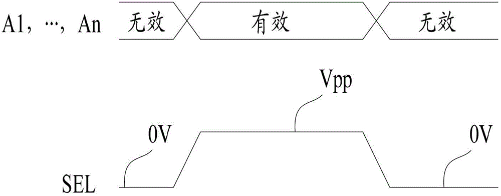
[0072] As described in Embodiment 1, when it is necessary to perform a write operation on the storage column controlled by the column decoding circuit, the amplitude of the column selection signal SEL rises from 0V to 7V-9V; When the storage column controlled by the decoding circuit performs a write operation, the amplitude of the column selection signal SEL drops from 7V-9V to 0V. During the rising and falling process of the amplitude of the column selection signal SEL, if the rate of change of the amplitude of the column selection signal SEL is too fast, it is easy to cause the transistors in the first driving circuit 44 and the second driving circuit 45 to generate Latch up (latch up) effect, resulting in transistor damage.

[0073] In order to solve the above problems, the technical solution of the present invention also provides Embodiment 2. Figure 7 It is a structural schematic diagram of the column decoding circuit of the memory according to Embodiment 2 of the prese...


PUM


Abstract

The invention discloses a storage and a column decoding circuit thereof. The column decoding circuit of the storage comprises a NAND gate circuit, a NOT gate circuit, a level shift circuit and a first driving circuit, which are connected in sequence, as well as a second driving circuit and a precharging circuit, wherein the second driving circuit comprises a first PMOS (P-channel Metal Oxide Semiconductor) tube, a first NMOS (N-channel metal oxide semiconductor) tube and a second NMOS tube; the precharging circuit comprises a second PMOS tube and a third NMOS tube; a source electrode of the second PMOS tube is suitable for being connected with a precharging power supply; and when the storage performs read operation, a voltage provided by the precharging power supply is a supply voltage of the storage. According to the storage and the column decoding circuit thereof provided by the technical scheme of the invention, the power consumption of the storage in reading operation can be reduced.

Description

technical field [0001] The invention relates to the technical field of memory, in particular to a memory and a column decoding circuit thereof. Background technique [0002] Memory (Memory) is a memory device in a computer system used to store programs and data. All information in the computer, including input raw data, computer programs, intermediate running results and final running results are stored in the memory. A memory contains many storage units. Usually, the storage units are arranged in an array, and each storage unit has an address corresponding to its position. When performing operations such as reading and writing to a certain storage unit in the storage array, the address needs to be decoded by the row decoding circuit and the column decoding circuit respectively, and the row and column where the storage unit is located are selected. [0003] figure 1 It is a schematic diagram of the structure of a common memory. refer to figure 1 , the memory includes a ...

Claims


Application Information

Patent Timeline
Patent Type & Authority Patents(China)
IPC IPC(8): G11C11/56
Inventor 杨光军
Owner SHANGHAI HUAHONG GRACE SEMICON MFG CORP
Why Eureka
Try Eureka