Trench gate power semiconductor device and method for manufacturing same

A technology of power semiconductors and trench gates, applied in semiconductor/solid-state device manufacturing, semiconductor devices, electrical components, etc. On-resistance, high reverse withstand voltage, and the effect of increasing impurity concentration

Active Publication Date: 2013-08-14
SHINDENGEN ELECTRIC MFG CO LTD
View PDF5 Cites 16 Cited by
  • Summary
  • Abstract
  • Description
  • Claims
  • Application Information

AI Technical Summary

Problems solved by technology

[0010] However, in the conventional trench gate power MOSFET900, due to the p + The existence of the buried region 940 will narrow the region where the

Method used


Image

  • Trench gate power semiconductor device and method for manufacturing same
  • Trench gate power semiconductor device and method for manufacturing same
  • Trench gate power semiconductor device and method for manufacturing same

Examples


Embodiment approach 1

[0040] 1. Trench gate power semiconductor device 100 of Embodiment 1

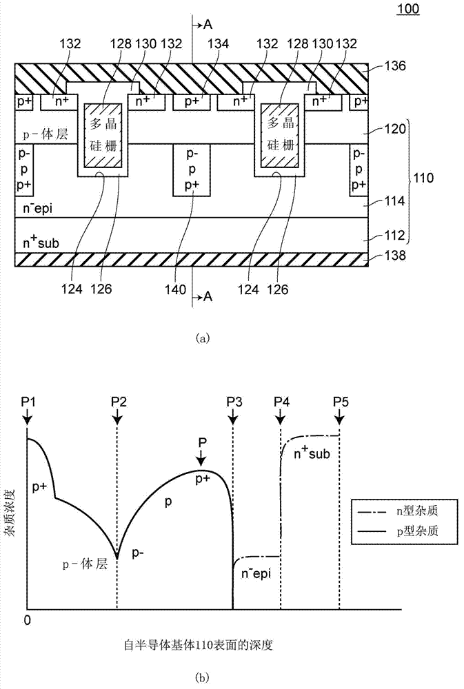
[0041] figure 1 It is an explanatory diagram showing the trench gate power semiconductor device 100 according to the first embodiment. figure 1 (a) is a cross-sectional view showing the trench gate power semiconductor device 100, figure 1 (b) is a schematic diagram showing concentration distributions of p-type impurities and n-type impurities in the trench gate power semiconductor device 100 .

[0042] Such as figure 1 As shown in (a), the trench gate power semiconductor device 100 of Embodiment 1 is a trench gate power MOSFET, which has: n -type drift layer 114; the p-type body layer 120 located on the drift layer 114; the body layer 120 is opened to reach the groove 124 formed by the drift layer 114; it is arranged in the body layer 120, and at least a part is placed on the inner periphery of the groove 124 n + type source region (first semiconductor region) 132; the gate insulating film 126 for...

Embodiment approach 2

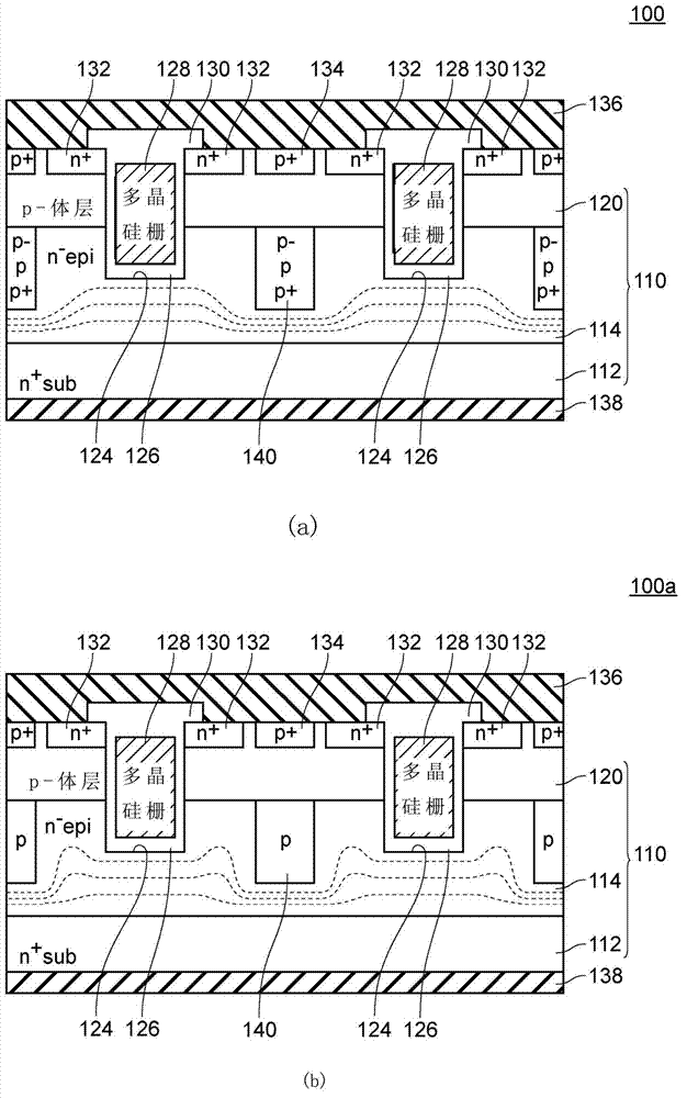
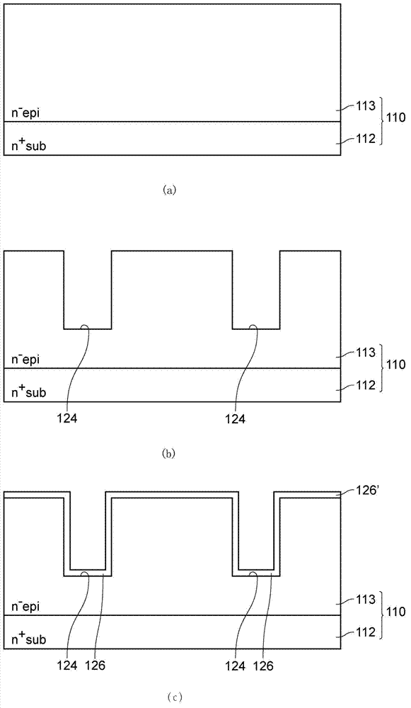
[0084] Figure 8 It is an explanatory diagram showing the trench gate power semiconductor device 102 according to the second embodiment. Figure 8 (a) is a cross-sectional view showing the trench gate power semiconductor device 102, Figure 8 (b) is a schematic diagram showing the concentration distribution of p-type impurities and n-type impurities in the trench gate power semiconductor device 102 . Figure 9 It is an explanatory diagram showing a method of manufacturing trench gate power semiconductor device 102 according to the second embodiment. Figure 9 (a)~ Figure 9 (c) is a schematic diagram showing the main works. in addition, Figure 9 (a) is with Figure 5 (a) The corresponding graph, Figure 9 (c) is with Figure 5 (b) Corresponding plot.

[0085] The trench gate power semiconductor device 102 of the second embodiment basically has the same structure as the trench gate power semiconductor device 100 of the first embodiment, but as Figure 8 As shown in FI...

Embodiment approach 3

[0091] Figure 10 It is a cross-sectional view showing the trench gate power semiconductor device 104 according to the third embodiment. The trench gate power semiconductor device 104 of the third embodiment basically has the same structure as the trench gate power semiconductor device 100 of the first embodiment, but the depth position of the bottom surface of the trench 124 is the same as that of the trench gate power semiconductor device of the first embodiment. The power semiconductor device 100 is different. That is, in the trench gate power semiconductor device 104 of the third embodiment, as Figure 10 As shown, the depth of the bottom of the groove 124 is deeper than the depth between the bottom of the bulk layer 120 and the bottom of the drift layer 114 .

[0092] In this way, although the trench gate power semiconductor device 104 of the third embodiment has a depth position of the bottom surface of the trench 124 that is different from the trench gate power semico...


PUM

PropertyMeasurementUnit
Thicknessaaaaaaaaaa
Thicknessaaaaaaaaaa
Thicknessaaaaaaaaaa

Abstract

A trench gate power semiconductor device (100) of the present invention is provided with: an n--type drift layer (114); a p-type body layer (120); a groove (124); an n+-type source region (132); a gate insulating film (126) that is formed on the inner peripheral surface of the groove (124); a gate electrode film (128) that is formed on the inner peripheral surface of the gate insulating film (126); and a source electrode layer (136) that is formed to be in contact with the source region (132), while being insulated from the gate electrode film (128). In the drift layer (114), a region sandwiched between two adjacent grooves (124) is provided with a p-type buried region (140) that is in contact with the body layer (120) and extends deeper than the grooves (124). In the buried region (140), the depth position at which the p-type impurity concentration is maximum is located deeper than the midway between the bottom surface (P2) of the body layer (120) and the bottom surface (P3) of the buried region (140). This trench gate power semiconductor device (100) has high reverse breakdown voltage and further lower on-resistance.

Description

technical field [0001] The invention relates to a trench gate power semiconductor device and a manufacturing method thereof. Background technique [0002] Conventionally, trench gate power MOSFETs have been widely used in various power supply devices such as DC-DC converters (for example, refer to Patent Document 1.). Figure 12 It is an explanatory diagram showing a conventional trench gate power MOSFET 900 . [0003] Conventional trench gate power MOSFET900, such as Figure 12 shown, with: n + type drain layer 912; the n on the drain layer 912 - type drift layer 914; the p-type body layer 920 located on the drift layer 914; the body layer 920 is opened to reach the groove 924 formed by the drift layer 914; it is arranged in the body layer 920, and at least a part is on the inner peripheral surface of the groove 924 exposed n + type source region 932; a gate insulating film 926 formed on the inner peripheral surface of the trench 924; a gate electrode layer 928 formed on...

Claims


Application Information

Patent Timeline
IPC IPC(8): H01L29/78H01L21/336H01L29/739
CPCH01L29/0878H01L29/66712H01L29/7397H01L29/1095H01L29/7813
Inventor 渡辺祐司岸雅人佐藤広輝竹森俊之丸岡道明
Owner SHINDENGEN ELECTRIC MFG CO LTD
Why Eureka
Try Eureka