Method for flattening thin film surface, array substrate and its preparation method, and display device

A surface planarization and array substrate technology, which is applied in semiconductor/solid-state device manufacturing, instruments, electrical components, etc., can solve problems such as surface flatness damage

Inactive Publication Date: 2016-01-06
BEIJING BOE OPTOELECTRONCIS TECH CO LTD
View PDF8 Cites 0 Cited by
  • Summary
  • Abstract
  • Description
  • Claims
  • Application Information

AI Technical Summary

Problems solved by technology

[0004] The invention provides a thin film surface planarization method, an array substrate and its preparation method, and a display device, which solves the technical problem that the existing dry etching greatly damages the flatness of other film layers below the etched film layer, Thereby improving the transmittance and contrast of LCD

Method used


Image

  • Method for flattening thin film surface, array substrate and its preparation method, and display device
  • Method for flattening thin film surface, array substrate and its preparation method, and display device
  • Method for flattening thin film surface, array substrate and its preparation method, and display device

Examples


Embodiment 1

[0038] The invention provides a processing method for flattening the surface of a thin film after dry etching. After pattern etching is performed on a non-metallic layer by dry etching, the surface of a first film layer exposed after dry etching is flattened. processing, so that the first film layer whose surface is rough due to dry etching is restored to be flat, and the first film layer is located under the non-metallic layer.

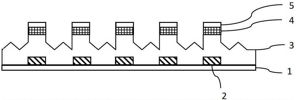
[0039] Dry etching is a pattern transfer method commonly used in the semiconductor field. It usually uses ion bombardment to bombard the film layer without photoresist (or other protective layer) protection, so that the film layer protected by photoresist will be bombarded. The pattern remains, but at the same time, it will damage the surface flatness of the first film layer below the etched film layer (when the first film layer is a non-metallic material, the damage is particularly serious), making the first film layer rough, Subsequent film formati...

Embodiment 2

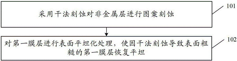
[0051] This embodiment provides a method for fabricating an array substrate, such as figure 1 As shown, the method includes:

[0052] 101. Pattern etching is performed on the non-metallic layer by dry etching, and after pattern etching is performed on the non-metallic layer by dry etching, the method further includes:

[0053] 102. Perform a surface planarization treatment on the first film layer, so that the first film layer whose surface is rough due to dry etching is restored to be flat, and the first film layer is located below the non-metallic layer.

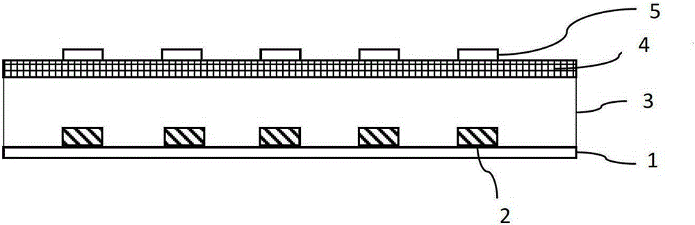
[0054] Wherein, the first film layer described in this embodiment is a general term for the film layer located under the etched film layer. For example, optionally, for an array substrate with a bottom gate structure, when the non-metallic layer is a semiconductor layer, the The first film layer is a gate insulating layer.

[0055] During the preparation of the array substrate, dry etching is often used to etch the non-me...


PUM


Abstract

The invention discloses a thin film surface planarization method, an array substrate and a preparation method thereof, and a display device, which relate to the display field and can solve the damage to the surface flatness of other film layers below the etched film layer by existing dry etching Large technical problems, thereby improving the display performance of liquid crystal displays. The method for preparing the array substrate of the present invention includes performing pattern etching on the non-metal layer by dry etching, and after performing pattern etching on the non-metal layer by dry etching, further includes: The layer is subjected to surface planarization treatment, so that the rough surface of the first film layer due to dry etching is restored to a flat surface, and the first film layer is located under the non-metallic layer.

Description

technical field [0001] The invention relates to the field of display, in particular to a method for flattening the surface of a thin film, an array substrate and a preparation method thereof, and a display device. Background technique [0002] Dry etching is a commonly used process in the field of semiconductor manufacturing. Usually, a radio frequency source is used to cause a plasma discharge phenomenon in the working gas to generate ions (Ion) and free radicals (Radical). These ions and free radicals act on the electric field. Next, ion bombardment is performed on the substance deposited on the substrate that is not covered by the photoresist, thereby transferring the pattern specified by the mask to the substrate. [0003] In the process of liquid crystal display array substrate processing, dry etching is generally used for pattern etching of non-metallic layers such as semiconductor layers, but dry etching usually adopts the form of ion bombardment to etch other layers ...

Claims


Application Information

Patent Timeline
Patent Type & Authority Patents(China)
IPC IPC(8): H01L21/306
CPCG02F1/136286G02F1/133357G02F1/136295H01L21/3065H01L21/308
Inventor 陈磊夏子祺代伍坤李嘉鹏金秀洪王凤国张磊仇淼
Owner BEIJING BOE OPTOELECTRONCIS TECH CO LTD
Why Eureka
Try Eureka