Semiconductor component coating film processing method

A semiconductor and component technology, applied in the field of coating process of semiconductor components, can solve problems such as component leakage, invisible cutting of the back-plated surface, and cracking of wafers, etc.

Inactive Publication Date: 2013-08-21
合肥彩虹蓝光科技有限公司
View PDF4 Cites 15 Cited by
  • Summary
  • Abstract
  • Description
  • Claims
  • Application Information

AI Technical Summary

Problems solved by technology

[0004] In the existing semiconductor LED manufacturing process, when the back is coated with a reflective film, if the back coating layer is impenetrable to the stealth dicing laser, during the process of crystal dicing, the reflection of the laser on the metal layer will cause Occurs when stealth dicing cannot be performed from the back-plated surface
When the back-plated reflective film layer contains metal, if the invisible cutting is performed from the front side of the crystal grain, that is, the non-back-plated surface, because the laser action is close to the LED epitaxial layer (EPI layer), it is easy to cause component leakage
In order to solve the problem that invisible dicing cannot be performed from the back-plated surface after the back-plated metal film layer, there is also a process that performs invi

Method used


Image

  • Semiconductor component coating film processing method
  • Semiconductor component coating film processing method

Examples


Embodiment Construction

[0030] The design method provided by the present invention is described in detail below by means of the accompanying drawings and specific examples:

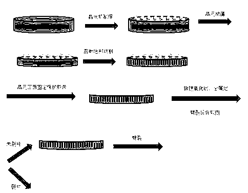
[0031] figure 1 It is a process diagram of semiconductor coating in the prior art, which includes the following steps:

[0032] 1) Thinning the wafer before the coating process;

[0033] 2) Stealth laser cutting of wafers;

[0034] 3) Fix the protective tape on the front of the wafer;

[0035] 4) Back plating oxide layer, metal layer;

[0036] 5) After the back plating is completed, the adhered and bonded substrates are peeled off;

[0037] 6) Split the unsplit pieces.

[0038] Due to the above-mentioned process, after the wafer is thinned for laser stealth dicing, the wafer is still fragile and difficult to handle only by adhesive tape, so it is prone to cracking, making the subsequent process difficult and not suitable for mass production.

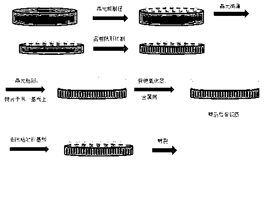
[0039] figure 2 It is a semiconductor coating process diag...


PUM


Abstract

The invention discloses a semiconductor component coating film processing method which includes a first step of conducting thinning on a wafer before conducting back coating on a reflective layer, a second step of conducting invisible laser cutting on the wafer, a third step of enabling the wafer which the invisible laser cutting is conducted on to be attached and bonded to a firm substrate, a fourth step of conducting the back coating on an oxidized layer or a metal layer, a fifth step of conducting peeling on the attached and bonded substrate after the back coating is completed, and a sixth step of conducting separation. Through addition of the process that the wafer is attached and bonded to the firm substrate, the semiconductor component coating film processing method solves the problems that in the prior art, the wafer is fragile and difficult to process and is easily broken when attached through only one adhesive tape after the invisible cutting.

Description

[0001] technical field [0002] The invention relates to the technical field of semiconductors, and more specifically, relates to a coating process method for semiconductor elements. [0003] Background technique [0004] In the existing semiconductor LED manufacturing process, when the back is coated with a reflective film, if the back coating layer is impenetrable to the stealth dicing laser, during the process of crystal dicing, the reflection of the laser on the metal layer will cause A situation where stealth dicing cannot be performed from the back-plated surface occurs. When the back-plated reflective film layer contains metal, if the invisible cutting is performed from the front side of the die, that is, the non-back-plated surface, since the laser action is close to the LED epitaxial layer (EPI layer), it is easy to cause component leakage. In order to solve the problem that invisible dicing cannot be performed from the back-plated surface after the back-p...

Claims


Application Information

Patent Timeline
IPC IPC(8): H01L21/683H01L33/00
Inventor 单立伟
Owner 合肥彩虹蓝光科技有限公司
Why Eureka
Try Eureka