

Thin film transistor liquid crystal display device and manufacturing method thereof
A technology for liquid crystal display devices and thin film transistors, which is applied in the manufacture of semiconductor/solid-state devices, semiconductor devices, electric solid-state devices, etc. Effect
- Summary
- Abstract
- Description
- Claims
- Application Information
AI Technical Summary
Problems solved by technology
Method used
Image

Examples
Embodiment Construction
[0070] In order to make the purpose, technical solutions and advantages of the embodiments of the present invention clearer, the technical solutions in the embodiments of the present invention will be clearly and completely described below in conjunction with the drawings in the embodiments of the present invention. Obviously, the described embodiments It is a part of embodiments of the present invention, but not all embodiments. Based on the embodiments of the present invention, all other embodiments obtained by persons of ordinary skill in the art without making creative efforts belong to the protection scope of the present invention.
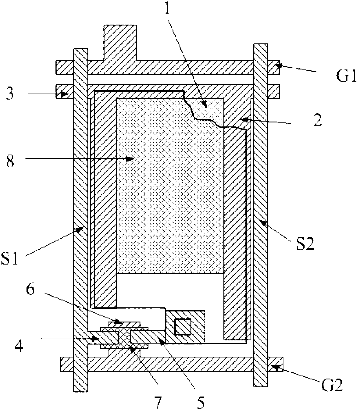
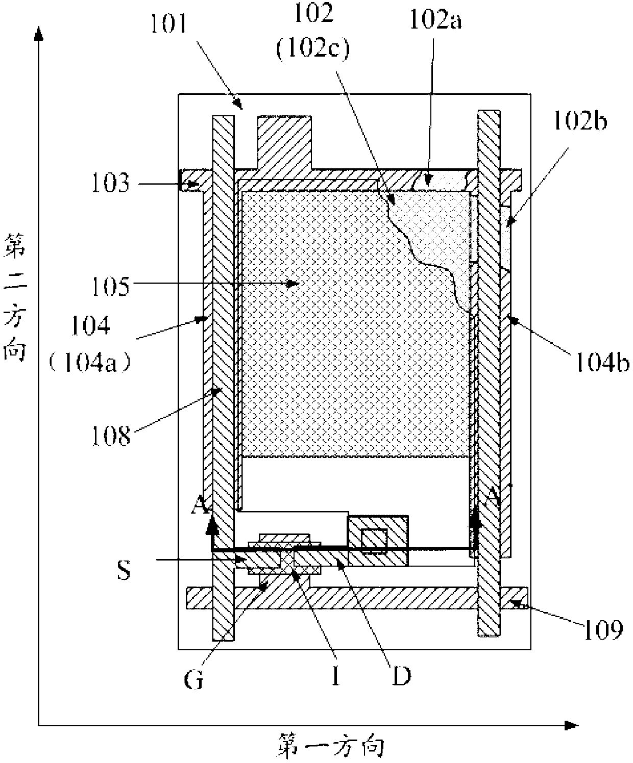
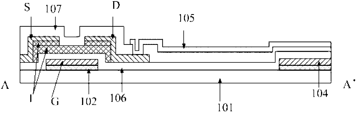
[0071] As mentioned in the background art, the existing thin film transistor liquid crystal display devices with transparent electrodes have a relatively low aperture ratio.
[0072] The inventor found that in order to reduce the load of the same chip, the existing liquid crystal display devices all have storage electrode lines, and a separat...
PUM
 Abstract
Description
Claims
Application Information