Display panel and display device

A display panel and display device technology, applied in the direction of electrical components, electric solid devices, circuits, etc., can solve the problems of uneven brightness, lower impedance, and insufficient driving current of the display device 1, so as to improve uneven brightness and reduce voltage. The effect of reducing, reducing complexity and its cost

Active Publication Date: 2013-09-11
INNOCOM TECH SHENZHEN +1
View PDF3 Cites 38 Cited by
  • Summary
  • Abstract
  • Description
  • Claims
  • Application Information

AI Technical Summary

Problems solved by technology

[0006] However, since the display device 1 emits light upwards, the common electrode layer 111 is a transparent electrode layer. Therefore, it needs to have good light transmittance, and is generally made of metals such as calcium, magnesium, lithium, silver, or alloy materials thereof, and In order not to affect the light transmission, the thickness of this layer is relatively thin, so the resistance is high
In order to reduce the impedance, a multi-layer film structure can be made of a light-transmitting metal oxide and the above metals or alloys, such as indium-tin oxide (ITO) or indium-zinc oxide (indium-zinc oxide) , IZO), but the impedance of this type of metal oxide material is still higher than that of metal, resulting in the impedance of the common electrode layer 111 being much higher than that of ordinary metal electrodes.
Therefore, in the case of a large-scale display device, when the driving signal is transmitted to, for example, the pixel P in the central area of ​​the display panel 11 through the wires 12 and 13, the voltage drop of the driving voltage will be too large because the impedance of the common electrode layer 111 is too large. High (that is, IR drop), resulting in insufficient driving current, and then causing uneven brightness of the display device 1 (such as the Mura phenomenon)
In addition, in the manufacturing process of making the organic light-emitting element E, the complexity of evaporating the organic light-emitting material is quite high, so that the cost of the display device 1 is also quite high.

Method used


Image

  • Display panel and display device
  • Display panel and display device
  • Display panel and display device

Examples


Embodiment Construction

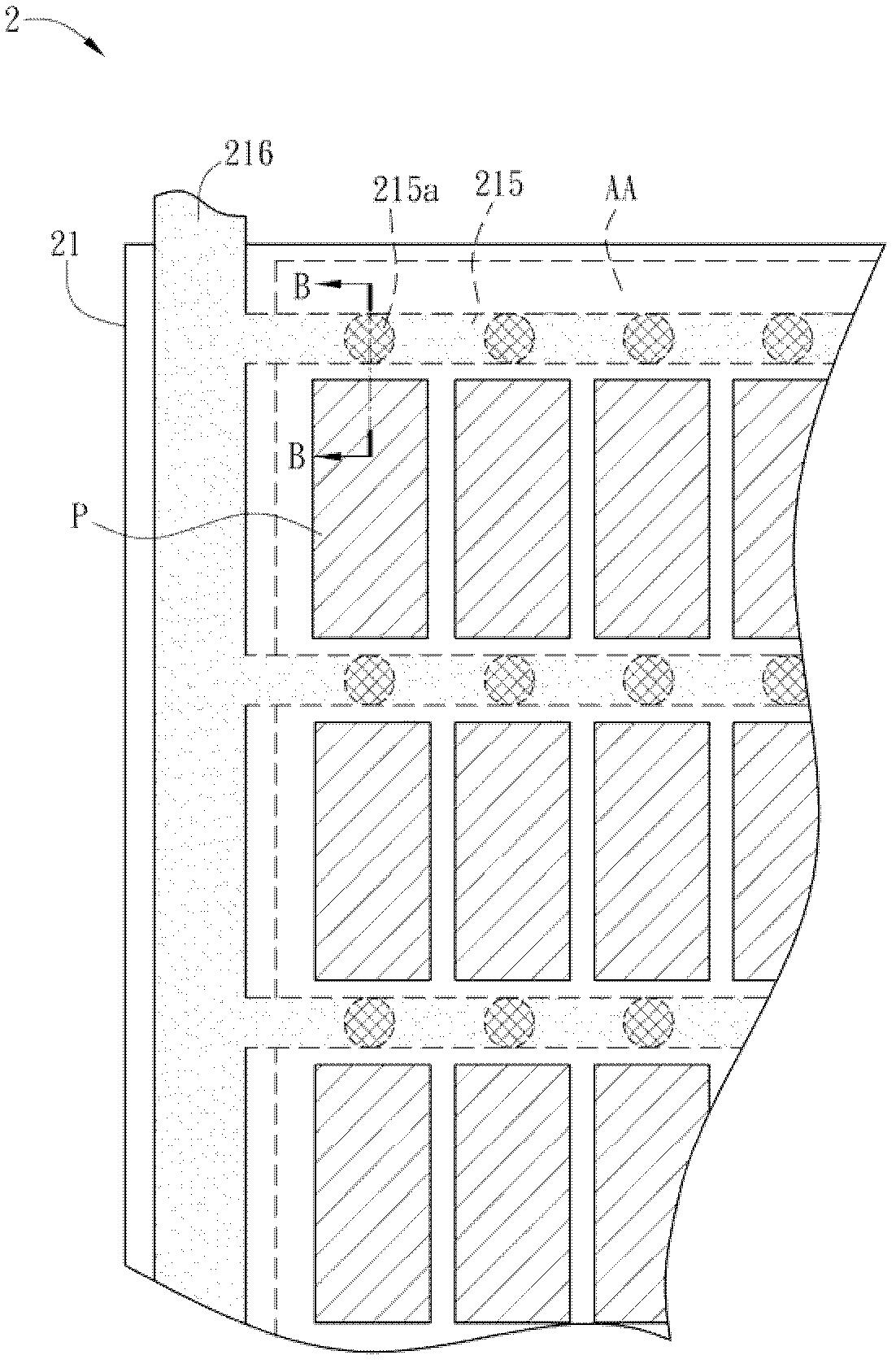
[0060] Please refer to Figure 2A and Figure 2B As shown, among them, Figure 2A is a partial schematic diagram of an organic light emitting display device 2, and Figure 2B for Figure 2A , the schematic cross-sectional view of the line B-B. Herein, an organic light emitting display device emitting upward light is taken as an example.

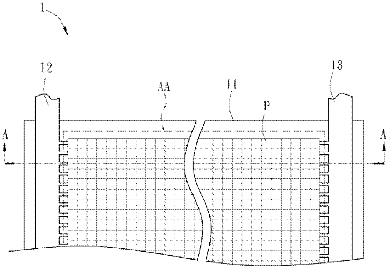
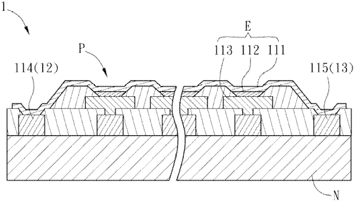
[0061] The display device 2 includes a display panel 21 , and the display panel 21 may have a display area AA for displaying image frames. In addition, the display panel 21 may include a plurality of pixels P disposed on a substrate N, and each pixel P may have an organic light emitting element E respectively. Such as Figure 2B As shown, the organic light emitting element E includes a pixel electrode layer 213 , an organic light emitting layer 212 and a common electrode layer 211 . The organic light emitting layer 212 is sandwiched between the pixel electrode layer 213 and the common electrode layer 211 to define the area size of the pi...


PUM


Abstract

The invention provides a display panel and a display device. The display panel comprises at least one pixel, an auxiliary electrode layer and a first organic material layer. The pixel comprises an organic light-emitting component which is provided with a first electrode layer. The auxiliary electrode layer is arranged adjacent to the pixel, and is provided with a through hole arranged corresponding to the pixel, the through hole is defined by a side wall of the auxiliary electrode layer, and the first electrode layer is electrically connected with the auxiliary electrode layer through the side wall. The first organic material layer is arranged in the through hole. The invention further discloses a display device with the display panel.

Description

technical field [0001] The present invention relates to a display panel and a display device, in particular to an organic light-emitting diode (Organic Light-Emitting Diode, OLED) display panel and a display device. Background technique [0002] Organic light-emitting diodes have the advantages of self-illumination, high brightness, high contrast, light and thin volume, low power consumption, and fast response. Therefore, they have been gradually applied to various display image systems, such as organic light-emitting display devices. Among them, organic light-emitting display devices can be divided into passive-matrix (Passive-Matrix) and active-matrix (Active-Matrix) according to their driving methods. Although the active matrix organic light emitting display device is more expensive and the manufacturing process is more complicated, it is suitable for full-color display with large size, high resolution and high information capacity, and it also saves power. Therefore, it ...

Claims


Application Information

Patent Timeline
Patent Type & Authority Applications(China)
IPC IPC(8): H01L27/32H01L51/52
Inventor 赵光品蔡旻翰黄浩榕
Owner INNOCOM TECH SHENZHEN
Why Eureka
Try Eureka