Micro-strip balanced filter
A balanced filter and filter technology, applied in the field of electronics, can solve the problems of low isolation, poor common mode noise suppression, and large system size of the balanced filter, and achieve the effects of compact structure, low insertion loss, and easy integration.
- Summary
- Abstract
- Description
- Claims
- Application Information
AI Technical Summary
Problems solved by technology
Method used
Image
Examples
Embodiment Construction
[0028] Below in conjunction with accompanying drawing, a kind of microstrip balanced filter that the present invention proposes is described in detail:
[0029] The output port and the input port of the balanced filter of the present invention are respectively welded with SMA heads, so as to be connected to testing or practical devices.
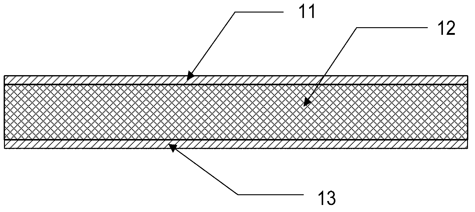
[0030] In this embodiment, a PCB board with a relative dielectric constant of 2.2 and a thickness of 0.508 mm is used as the substrate, and a PCB board of other specifications may also be used as the substrate. Such as figure 1 As shown, the upper and lower surfaces of the dielectric substrate 12 of the PCB are respectively covered with an upper metal patch 11 and a lower metal patch 13 .
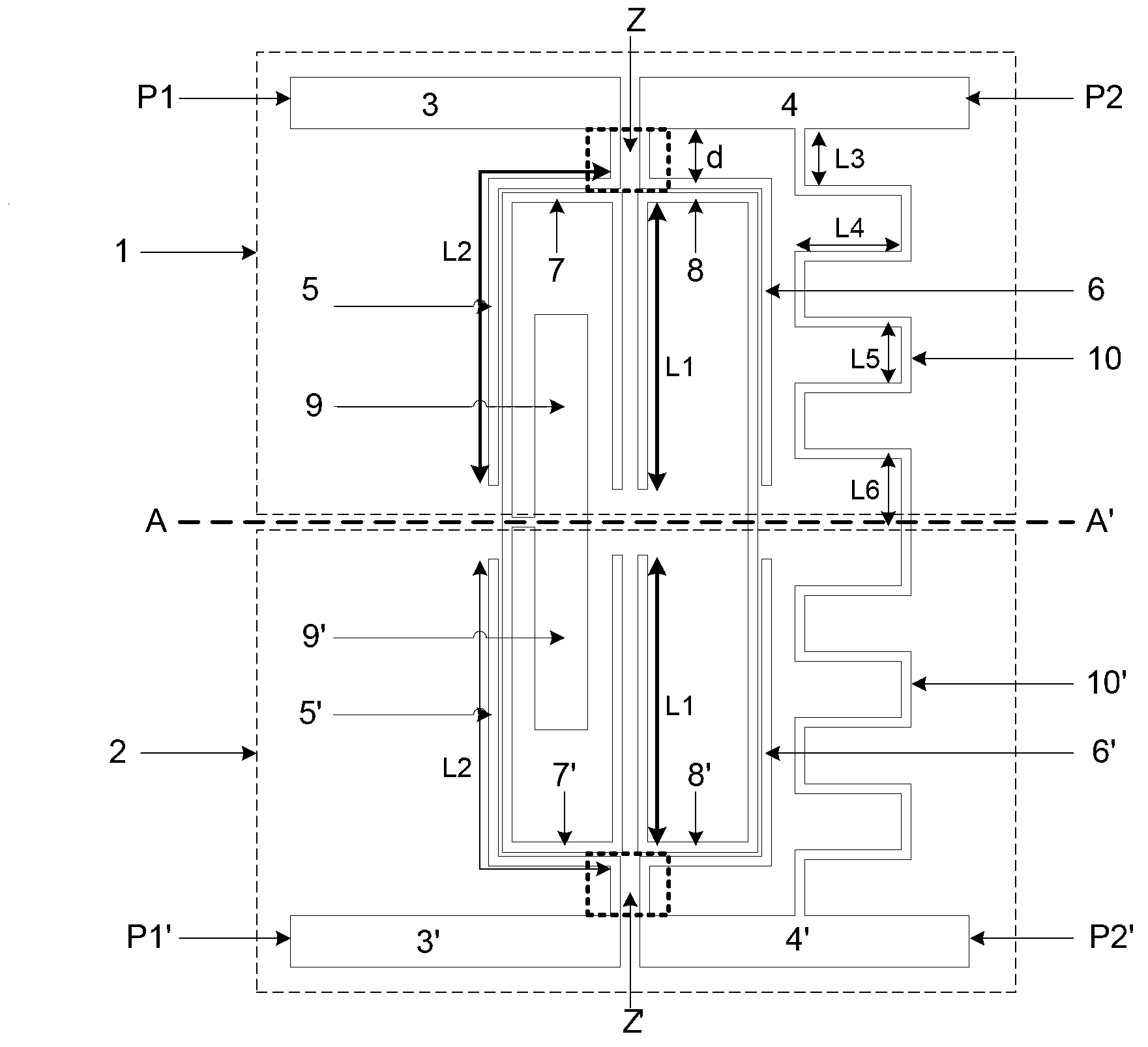
[0031] Such as figure 2 As shown, the balanced filter of the present invention is formed on the PCB board and consists of two microstrip filters, which are respectively the first filter 1 and the second filter 2; the first filter 1 and the second filter...
PUM
| Property | Measurement | Unit |
|---|---|---|
| Impedance | aaaaa | aaaaa |
Abstract
Description
Claims
Application Information


