Chemical mechanical polishing (CMP) device and system
A technology of chemical machinery and grinding devices, which is applied in the direction of grinding devices, grinding machine tools, grinding/polishing equipment, etc., can solve the problems of removing uneven thickness, reducing wafer scrap rate, etc., and achieve good inter-wafer uniformity, effective Conducive to heat dissipation, remove the effect of uniform thickness
- Summary
- Abstract
- Description
- Claims
- Application Information
AI Technical Summary
Problems solved by technology
Method used
Image

Examples
Embodiment 1
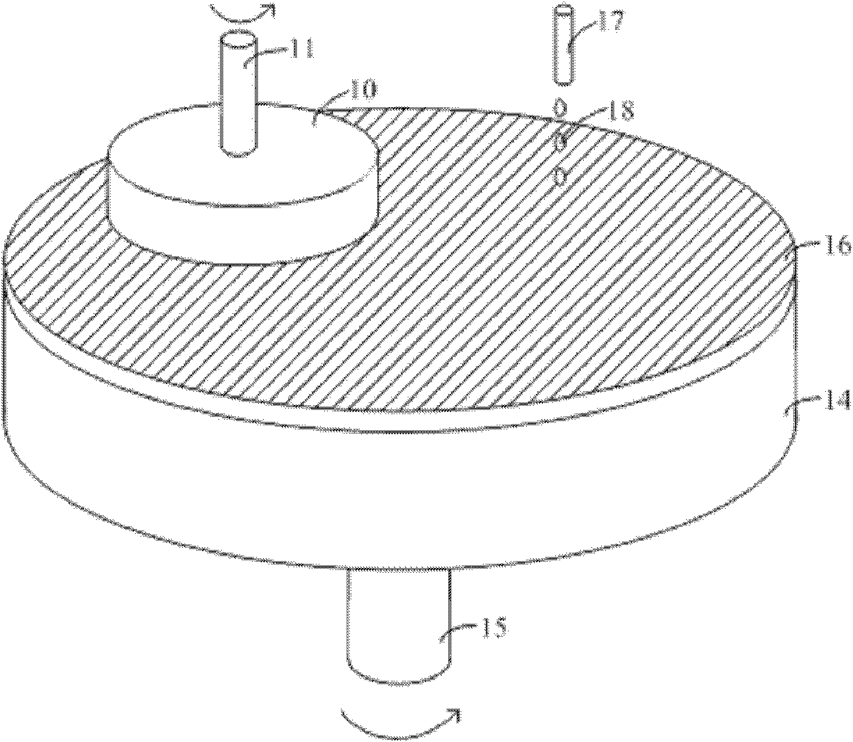
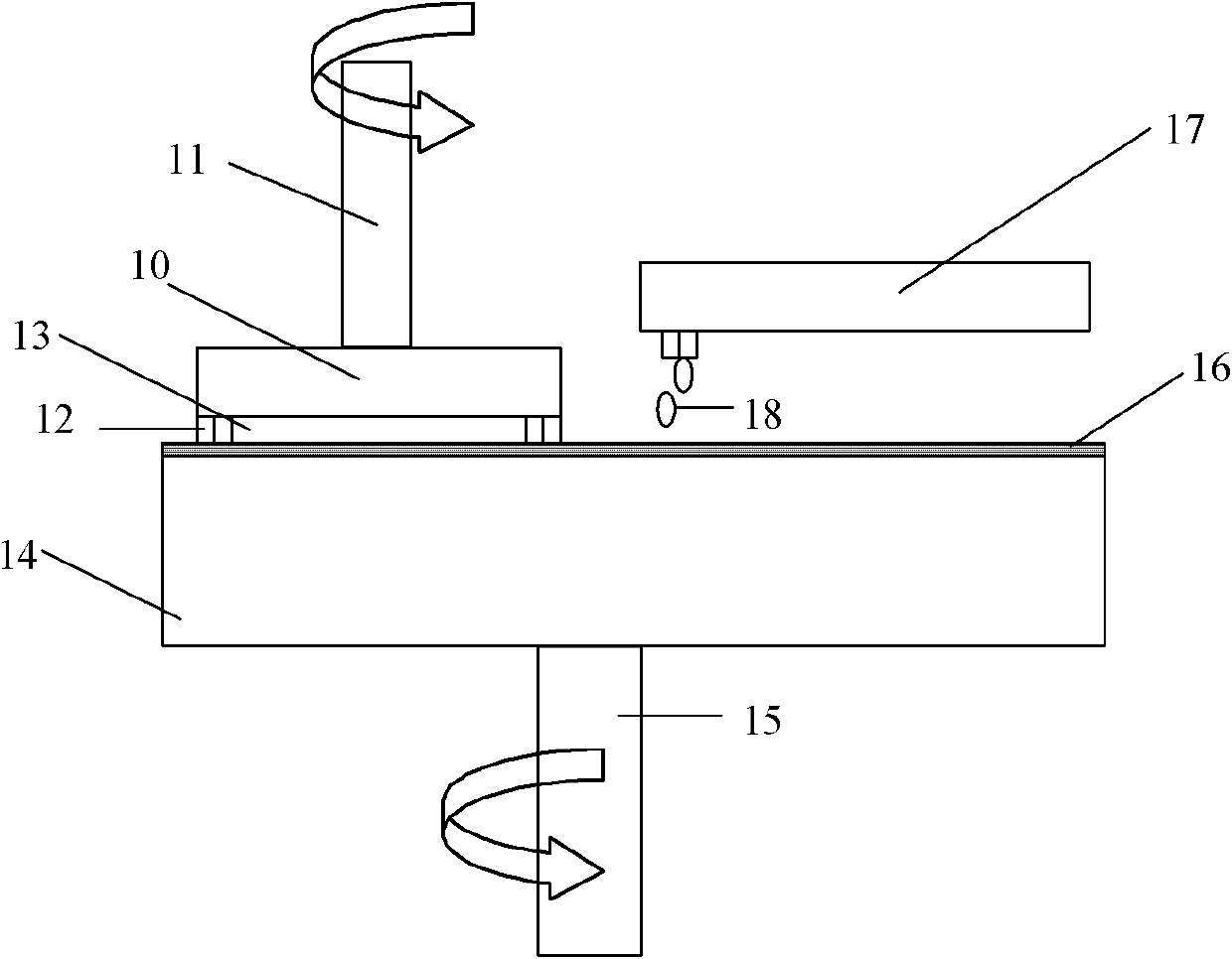
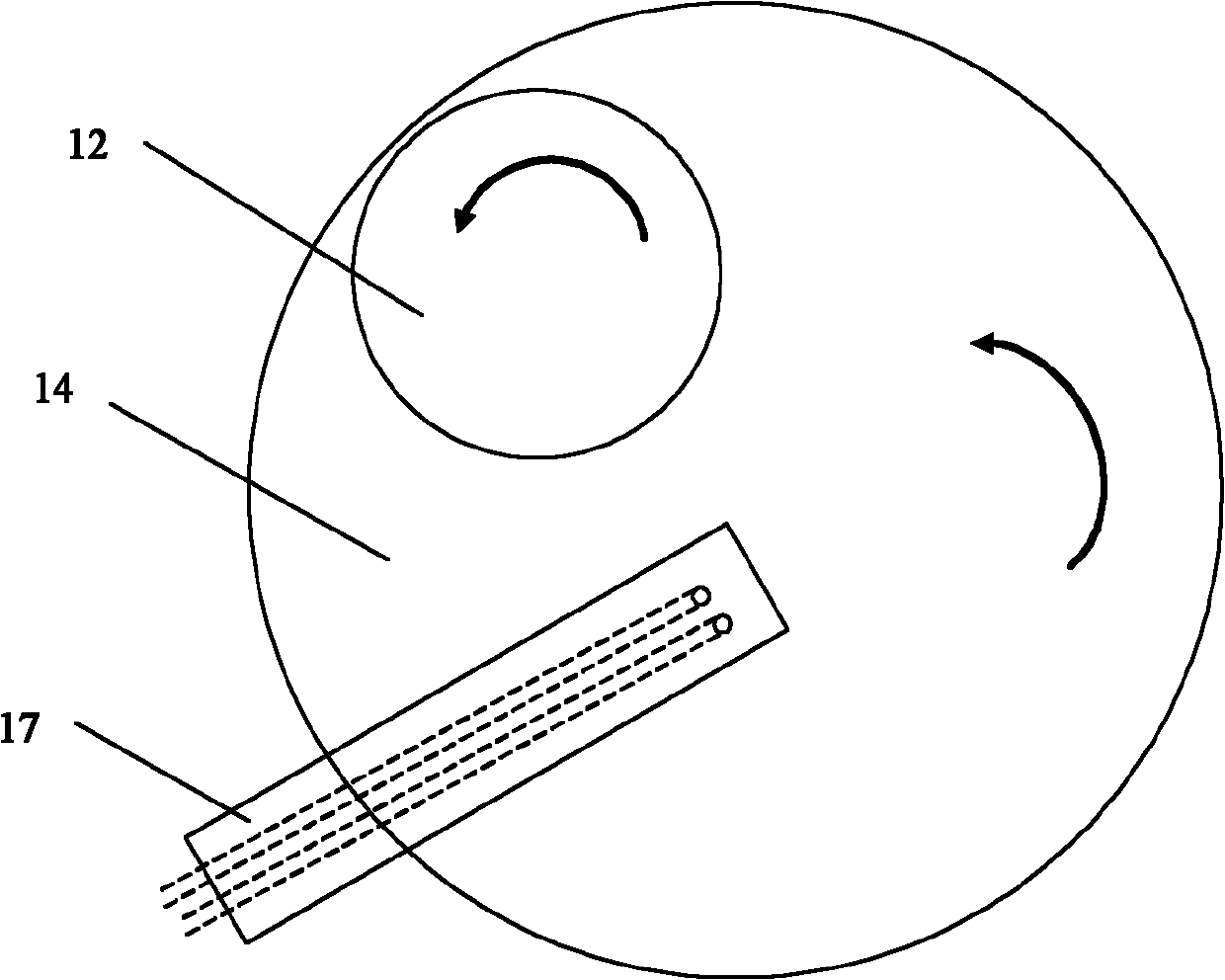
[0056] Figure 4 It is a cross-sectional view of the chemical mechanical polishing device provided in Embodiment 1; Figure 5 It is an enlarged schematic diagram of the heat dissipation device in Embodiment 1; Image 6 It is a schematic plan view of the cooling device in Embodiment 1; in combination with Figure 4 , Figure 5 with Image 6 , the chemical mechanical grinding device comprises:
[0057] polishing table 24;
[0058] A polishing pad 26 fixed above the polishing table 24;
[0059] Polishing head 20, the end face of described polishing head 20 cooperates with described polishing pad 26, is used for grinding wafer 23;
[0060] The clamping ring 22 is arranged on the edge of the end face of the polishing head 20 to clamp the wafer 23, and the thickness of the clamping ring 22 is equal to or smaller than the thickness of the wafer 23;
[0061] Shaft 21, arranged above the polishing head 20, is used to drive the polishing head 20 to rotate and move;
[0062] The ...
Embodiment 2
[0074] The following is the second embodiment of the present invention, which is different from the structure in which the cooling device is arranged on the outside of the polishing head in the previous embodiments. In the second embodiment, the cooling device of the chemical mechanical polishing device is a cooling chamber, which is arranged on the polishing Pad 36 and polishing table 34 (see Figure 7 )between.
[0075] Figure 7 is a schematic cross-sectional view of the chemical mechanical polishing device provided in Example 2; Figure 8 is a schematic cross-sectional view of the heat sink in Embodiment 2; Figure 9 yes Figure 8 A schematic plan view of the cooling device; Figure 10 yes Figure 8 A side view of the heat sink.
[0076] combine Figure 7 with Figure 8 , in this embodiment, the chemical mechanical polishing device includes a polishing table 34, a polishing pad 36, a polishing head 30, a clamping ring 32, a shaft 31, a transmission member 35, a pip...
Embodiment 3
[0085] The following is the third embodiment of the present invention. Different from the previous two examples, such as Figure 11 As shown, the chemical mechanical grinding device of the third embodiment is provided with a first heat dissipation device 49 on the outside of the polishing head 40, and a heat dissipation chamber 59 is set between the polishing pad 46 and the polishing table 44 (the second cooling device). The first heat dissipation device 49 may be the same as that in Embodiment 1, and the second heat dissipation device 59 may be the same as that in Embodiment 2. Please refer to Embodiment 1 and Embodiment 2 for specific structures.
[0086] The present invention also provides a chemical mechanical polishing system, comprising:
[0087] 1 or more chemical mechanical grinding devices as described in embodiments one to three;
[0088] 1 or more cleaning chambers;
[0089] 1 or more transfer devices.
[0090] The cleaning chamber is used for cleaning the wafe...
PUM
| Property | Measurement | Unit |
|---|---|---|
| Spacing | aaaaa | aaaaa |
Abstract
Description
Claims
Application Information
 - R&D
- Intellectual Property
- Life Sciences
- Materials
- Tech Scout
- Unparalleled Data Quality
- Higher Quality Content
- 60% Fewer Hallucinations
Browse by: Latest US Patents, China's latest patents, Technical Efficacy Thesaurus, Application Domain, Technology Topic, Popular Technical Reports.
© 2025 PatSnap. All rights reserved.Legal|Privacy policy|Modern Slavery Act Transparency Statement|Sitemap|About US| Contact US: help@patsnap.com