Simulation device of load data processor and implementation method thereof

A load data and simulation device technology, applied in the field of satellite testing, can solve problems such as the difficulty in fault location of satellite data transmission subsystems, and achieve the effects of improving test efficiency, reducing test costs, and improving safety and reliability

Active Publication Date: 2013-09-18
HARBIN INST OF TECH
View PDF2 Cites 22 Cited by
  • Summary
  • Abstract
  • Description
  • Claims
  • Application Information

AI Technical Summary

Problems solved by technology

[0004] The purpose of the present invention is to solve the problem of difficult fault location in the testing process of the existing satellite data transmission subsystem, and to provide a simulation device of a load data processor and its implementation method

Method used


Image

  • Simulation device of load data processor and implementation method thereof
  • Simulation device of load data processor and implementation method thereof
  • Simulation device of load data processor and implementation method thereof

Examples


specific Embodiment approach 1

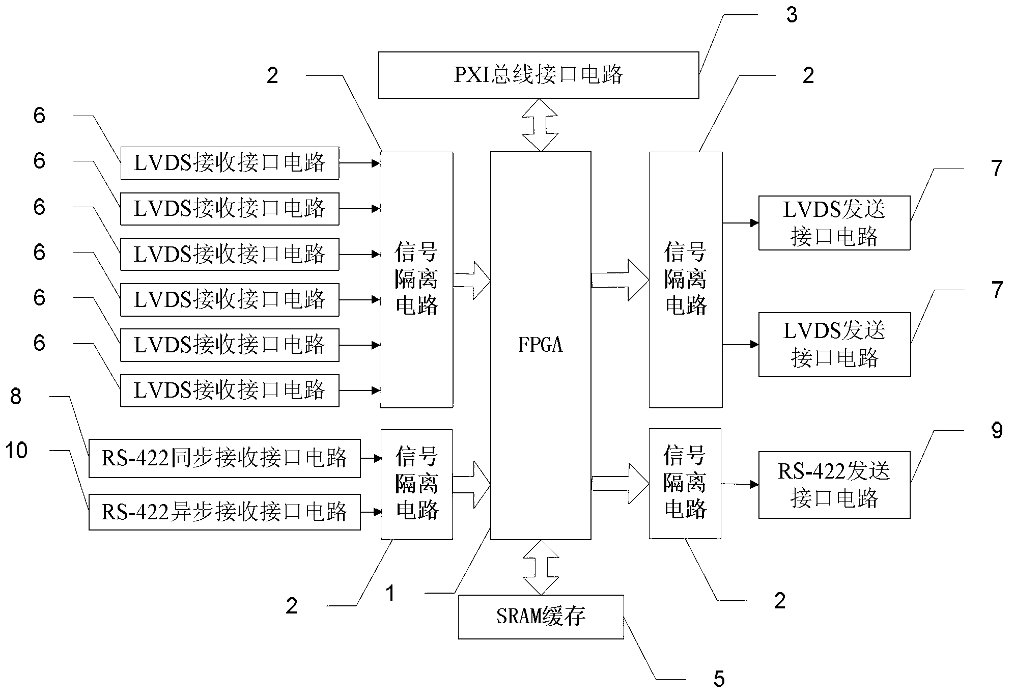
[0028] Specific implementation mode one: the following combination figure 2 Describe the present embodiment, the load data processor simulation device described in the present embodiment, it comprises FPGA1, signal isolation circuit 2, PXI bus interface circuit 3, LVDS receiving and sending interface circuit and RS-422 data receiving and sending circuit, described The LVDS receiving and sending interface circuit includes 6 LVDS receiving interface circuits 6 and 2 LVDS sending interface circuits 7, and the RS-422 data receiving and sending circuit includes 1 RS-422 synchronous receiving interface circuit 8, 1 RS-422 Asynchronous receiving interface circuit 10 and 1 RS-422 sending interface circuit 9,

[0029] The high-speed data signal output terminals of the 6 LVDS receiving interface circuits 6 are respectively connected to the high-speed data signal input terminals of the first signal isolation circuit 2, and the high-speed data signal output terminals of the first signal ...

specific Embodiment approach 2

[0033] Specific implementation mode two: the following combination figure 2 Describe this embodiment mode, this embodiment mode will further explain Embodiment 1, and it also includes SRAM cache 5, and the buffer data input and output end of FPGA1 is connected to the buffer data input and output end of SRAM cache 5.

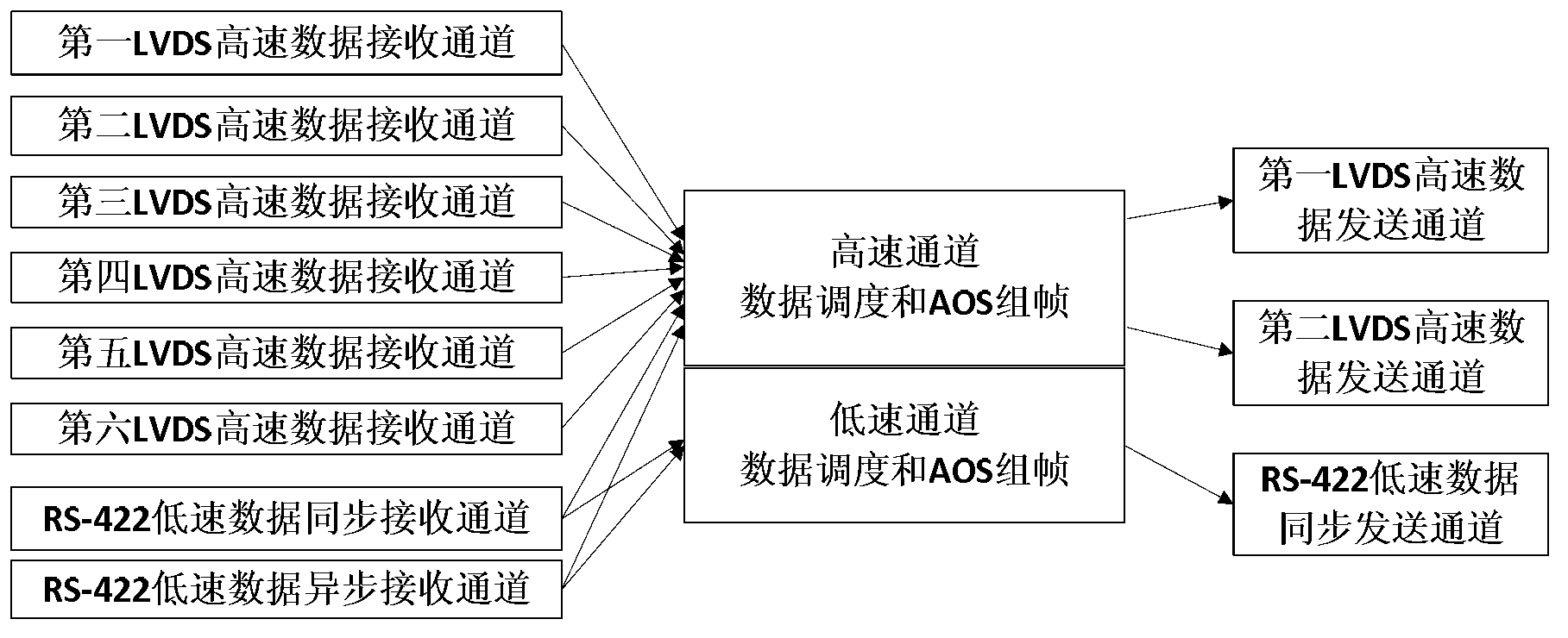
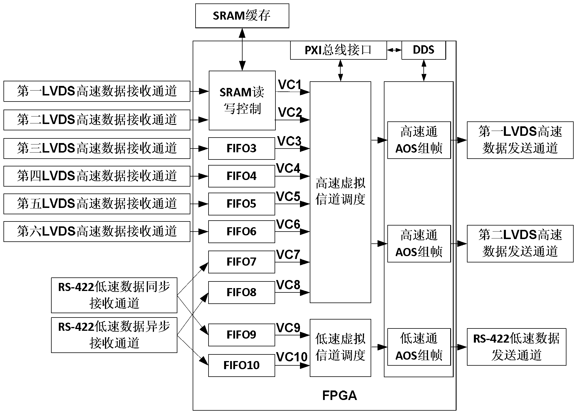
[0034] In this embodiment, the load data of most channels can be cached by the FPGA internal FIFO, and the load data of individual large-capacity and high-speed channels need to pass through the SRAM cache 5 to avoid frame loss. After the cached data is scheduled and framed by AOS, the The LVDS receiving and sending interface circuit and the RS-422 synchronous data receiving circuit send out.

specific Embodiment approach 3

[0035] Embodiment 3: This embodiment further describes Embodiment 1. The transmission rate of the LVDS receiving and sending interface circuit is greater than or equal to 96 Mbps.


PUM


Abstract

The invention relates to a simulation device of a load data processor and an implementation method thereof, and belongs to the field of satellite test. The invention aims to solve the problems of high cost, low test safety and reliability and low test efficiency caused by that the test process of the existing satellite data transmission subsystem is performed in the sky. The simulation device of the load data processor comprises a field programmable gate array (FPGA), a signal isolation circuit, a PXI bus interface circuit, a low voltage differential signaling (LVDS) receiving and transmitting interface circuit and an RS-422 data receiving and transmitting circuit, wherein the LVDS receiving and transmitting interface circuit comprises an LVDS receiving interface circuit and an LVDS transmitting interface circuit; and the RS-422 data receiving and transmitting circuit comprises an RS-422 synchronous receiving interface circuit, an RS-422 asynchronous receiving interface circuit and an RS-422 transmitting interface circuit. The simulation device of the load data processor also comprises a static random access memory (SRAM) cache. The simulation device of the load data processor is applied to test of a satellite data transmission subsystem.

Description

technical field [0001] The invention relates to a simulation device of a load data processor and a realization method thereof, belonging to the field of satellite testing. Background technique [0002] In the satellite data transmission subsystem, with the development of satellite technology, the payload data presents the characteristics of many transmission channels, a large amount of one-way transmission data, and a high code rate. Orbit System (AOS), which provides a solution for large-capacity, high-speed broadband data communication requirements. The payload data processor is an important part of the satellite data transmission subsystem. It adopts the AOS specification proposed by CCSDS to complete the interweaving, combining, framing and distribution of multi-channel payload data, and realize multi-channel, large-capacity, and high-speed payload data. transmission with high reliability. [0003] The existing payload data processor is generally connected with the sat...

Claims


Application Information

Patent Timeline
Patent Type & Authority Applications(China)
IPC IPC(8): G06F11/22G06F9/455
Inventor 赵光权乔立岩彭宇刘月峰杨兆君王超
Owner HARBIN INST OF TECH
Why Eureka
Try Eureka