Pixel circuit, driving method thereof and pixel array structure

A pixel circuit and circuit technology, applied in static indicators, instruments, etc., can solve the problems of suppressing large-scale application of current-type drive circuits, long charging time of capacitors, and affecting display, etc.

Active Publication Date: 2013-09-18
BOE TECH GRP CO LTD
View PDF6 Cites 10 Cited by
  • Summary
  • Abstract
  • Description
  • Claims
  • Application Information

AI Technical Summary

Problems solved by technology

A major defect of this type of current-mode drive pixel circuit is that the charging time of the capacitor is too long, which affects the display and inhibits the large-scale application of the current-mode drive circuit.

Method used


Image

  • Pixel circuit, driving method thereof and pixel array structure
  • Pixel circuit, driving method thereof and pixel array structure
  • Pixel circuit, driving method thereof and pixel array structure

Examples


Embodiment 1

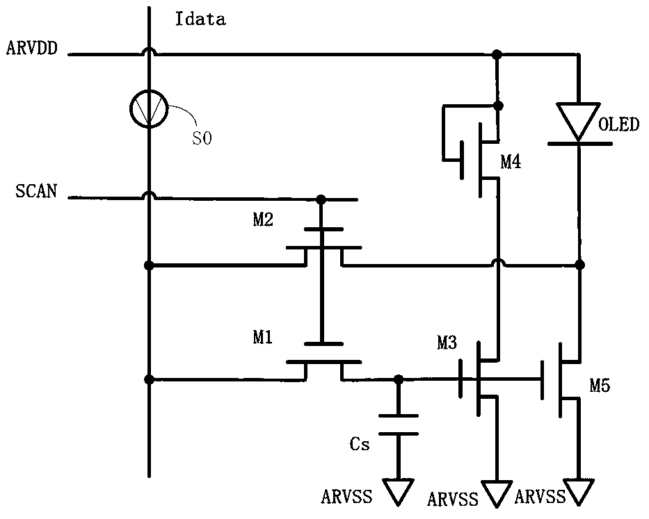
[0065] In Embodiment 1, all TFTs are N-type TFTs, all N-type TFTs are turned on at high level and turned off at low level, the first power supply is the negative power supply VSS, and the second power supply is the positive power supply VDD. And preferably, the data signal line is provided with a data signal by a semi-digital current source, and the following embodiments are the same, and will not be repeated here.

[0066] Such as Figure 5 As shown, a pixel circuit 1 provided by an embodiment of the present invention includes: a load control module 101, a load module 102, a grayscale selection module 103, a driving module 104, and a light emitting element 105, wherein,

[0067] The load control module 101 is connected to the first scan signal line scan1 and the data line Idata, is controlled by the first scan signal, and outputs an analog data signal through the first node A1 and the second node A2;

[0068] The load module 102 is respectively connected to the first power s...

Embodiment 2

[0094] Different from Embodiment 1, in Embodiment 2 of the present invention, the load module 102 further includes a fourth thin film transistor T104, wherein the gate and source of the fourth thin film transistor T104 are connected to the second power supply terminal VDD, and the drain is connected to the second power supply terminal VDD. Three nodes A3, such as Figure 7 shown.

[0095] The driving method in Embodiment 2 of the present invention is different from the pixel circuit in Embodiment 1 in that:

[0096] The third stage: T104 is turned on to prevent T103 from entering the deep linear region and preventing the drop of the drain voltage of T103 from interfering with the gate voltage of T103, so as to ensure that T103 can work in the saturation region and provide the seventh TFT T107 and the eighth TFT T108 current.

[0097] Therefore, the addition of the fourth thin film transistor optimizes the structure of the pixel circuit.

[0098] The simulation result of emb...

Embodiment 3

[0100] The difference from Embodiment 1 is that all TFTs in Embodiment 3 of the present invention are P-type TFTs, and they are all turned on at low level and turned off at high level. The first power supply is the positive power supply VDD, and the second power supply is the negative power supply. VSS. The structure of the pixel circuit described in Embodiment 2 is as follows Figure 9 As shown, its timing diagram is shown in Figure 10 As shown, so its driving method includes:

[0101] The pixel circuit driving method provided in Embodiment 3 of the present invention includes:

[0102] The first stage T11: the first scan signal scan1 is at low level, the second scan signal scan2 is at high level, the second power supply terminal VSS outputs high level, and the data signal line outputs an analog data signal, and the load control module 101 will The analog data signal is transmitted to the load module 102, and the analog data signal is stored in the load module 102, and the...


PUM


Abstract

The invention discloses a pixel circuit, a driving method thereof and a pixel array structure, aiming to reduce charging time of an OLED (organic light emitting diode) pixel circuit. The pixel circuit comprises a load control module, a load module, a gray scale selection module, a driving module and a light emitting element. The load control module is controlled by a first scanning signal line to store data signals at a first node and a second node. The load module is connected with a first power supply terminal, the driving module, the first node and the second node respectively, and is controlled by the first node signal and the second node signal to store analog data signals at the load module and provide the analog data signals to the driving module. The gray scale selection module is controlled by a second scanning signal line to transmit digital data signals to a third node of the gray scale selection module. The driving module is controlled by the second node signal and a third node signal to drive the light emitting element. The first end of the light emitting element is connected with a second power supply terminal while the second end of the same is connected with the driving module.

Description

technical field [0001] The present invention relates to the field of display technology, in particular to a pixel circuit, a driving method, and a pixel array structure. Background technique [0002] The brightness of organic electroluminescent display OLED is directly proportional to the driving current passing through it, so the pixel circuit must provide a continuous and stable driving current for the entire frame period. At present, OLED pixel circuit driving methods can be divided into current driving and voltage driving, respectively as figure 1 and figure 2 shown. [0003] In the voltage drive circuit, the current I flowing through the light-emitting element oled for: [0004] I OLED = 1 2 μ n · Cox · W L · ( Vdata - ...

Claims


Application Information

Patent Timeline
Patent Type & Authority Applications(China)
IPC IPC(8): G09G3/32
CPCG09G3/3233G09G2300/043G09G2300/0819
Inventor 段立业王俪蓉吴仲远
Owner BOE TECH GRP CO LTD
Why Eureka
Try Eureka