Chip packaging and testing device and lead frame used therefor

A testing device and chip packaging technology, applied in semiconductor/solid-state device testing/measurement, electrical components, electrical solid-state devices, etc., can solve problems such as unreasonable design size of the injection channel, waste of lead frame materials, and impact on work efficiency, etc. Achieve the effect of improving parallel testing efficiency, increasing rigidity, and improving utilization

Active Publication Date: 2016-04-13
SHENZHEN STS MICROELECTRONICS CO LTD
View PDF3 Cites 4 Cited by
  • Summary
  • Abstract
  • Description
  • Claims
  • Application Information

AI Technical Summary

Problems solved by technology

[0010] 1) The ratio of the effective chip area to the entire lead frame is too low (accounting for only 55.7% of the total area), and other parts are used as scraps and eventually discarded, which directly leads to the waste of lead frame materials
[0011] 2) The unreasonable design size of the injection channel leads to a serious waste of molding resin at the molding station. For the process based on the whole frame (such as molding, etc.), the number of products that can be effectively worked at one time is only 120 capsules, which greatly affects the work efficiency of the corresponding station

Method used


Image

  • Chip packaging and testing device and lead frame used therefor
  • Chip packaging and testing device and lead frame used therefor
  • Chip packaging and testing device and lead frame used therefor

Examples


Embodiment Construction

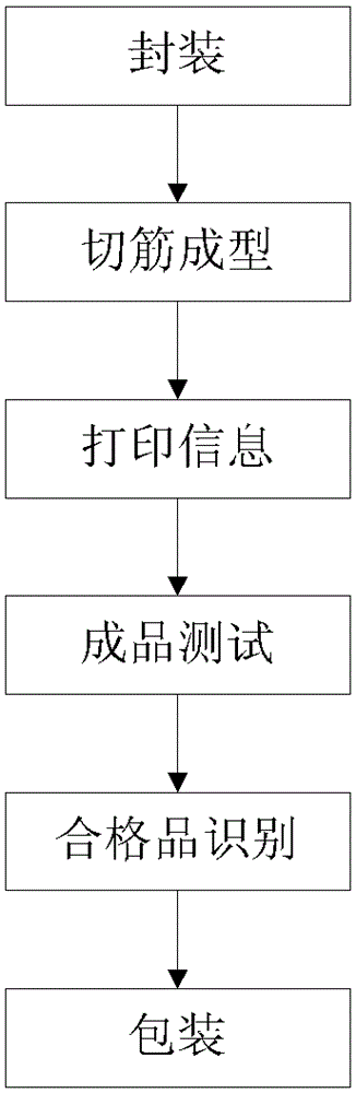
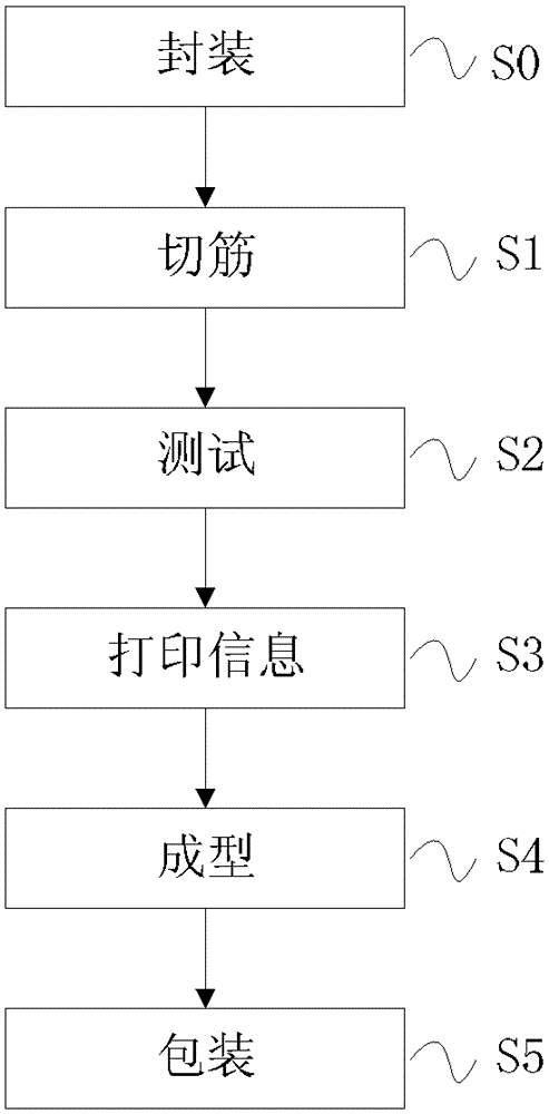
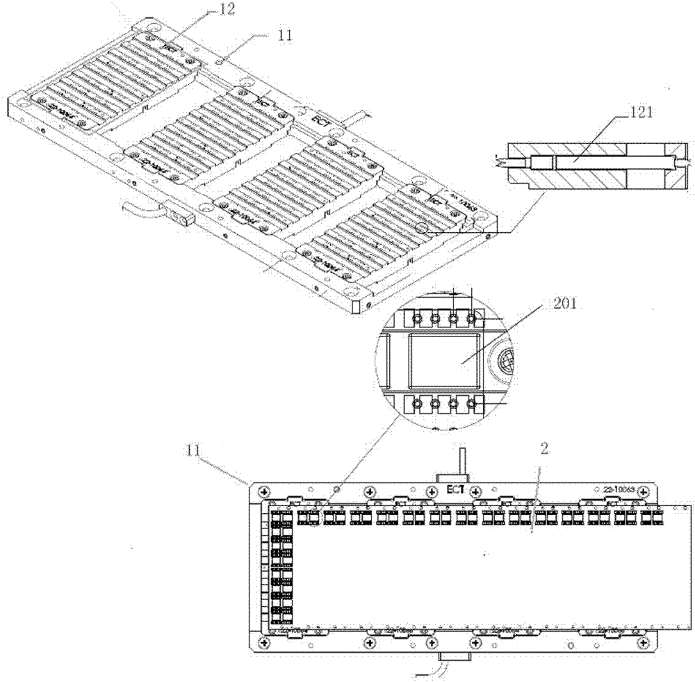
[0034] The present invention optimizes the STRIPTEST test method by developing a chip packaging and testing device with a higher density of packaging units and its dedicated lead frame, that is, it adopts two-dimensional code recognition technology or barcode technology, network technology and database technology, and ensures the smoothness of the test process. Safe, intelligent, and efficient, greatly improving the dependence of testing on manual operation and the potential risk of mixing related to it; at the same time, in order to give full play to the efficiency of the STRIPTEST system, the design of the lead frame is specially improved, and the unit frame is doubled. Density and number of packaged units.

[0035] The specific embodiment of the present invention will be further described in detail below in conjunction with the accompanying drawings.

[0036] It should be noted that, compared with the traditional packaging and testing process, STRIPTEST puts more emphasis o...


PUM


Abstract

Disclosed are a chip package testing device and a lead frame used thereby. The device comprises a test processing unit, a contactor bracket and a plurality of contactor units. The lead frame is fixedly arranged on the contactor bracket. Each contactor unit is provided with a probe array composed of a plurality of contact probes, the spacing size of the contactor probes is transversely and longitudinally matched with the spacing size of pins of packaged chips on the lead frame, the contact probes are arranged on the contactor bracket in a platform contact method and are electrically connected with the pins of the packaged chips, and the number of the packaged chips is an integral multiple of the number of the contact probes contained in the contact probe arrays. An injection-molding rubber channel on the lead frame includes a plurality of capsule-shaped slots, wherein a connection gap between every two capsule-shaped slots is located in the position of one chip pin, the capsule-shaped slots are located in the end parts of the chips and are in one-to-one correspondence with the chips, and the injection-molding rubber channel is located on the upper surface of the lead frame. According to the invention, the efficiency of parallel test is improved, and the utilization rate of the lead frame and mold sealing materials is improved.

Description

technical field [0001] The invention relates to the field of semiconductor chip packaging, in particular to a semiconductor chip packaging and testing device and a lead frame used therefor. Background technique [0002] The post-test packaging process of traditional semiconductor chips includes: packaging process→ribbon cutting and molding→printing information→finished product testing→qualified product identification→packaging, such as figure 1 shown. Among them, the finished product testing station separates defective products through automatic testing equipment, so as to ensure that only qualified products are sent to the packaging station and customers. Qualified product identification, that is, chip selection, is to discard the chips (marked with ink dots) that are tested as bad products on the wafer through image recognition technology, and only grab the chips that pass the test and mount them on the lead frame. [0003] The traditional chip packaging and testing meth...

Claims


Application Information

Patent Timeline
Patent Type & Authority Patents(China)
IPC IPC(8): H01L21/66H01L23/495
CPCH01L2224/97
Inventor 张萍匡秋红李现勇宋恩琳张云超喻宁王艳杨浩
Owner SHENZHEN STS MICROELECTRONICS CO LTD
Why Eureka
Try Eureka