Detection device and method for LED chip and device

A technology of LED chips and detection devices, which is applied in the direction of single semiconductor device testing, etc., can solve the problems of restricting the cost of LED devices, the number of operations of equipment mechanism, and the complexity of the system, so as to improve the competitive advantage of product cost, good industrialization prospects, and improve The effect of detection efficiency

Active Publication Date: 2013-09-25
SOUTH CHINA UNIV OF TECH
View PDF5 Cites 17 Cited by
  • Summary
  • Abstract
  • Description
  • Claims
  • Application Information

AI Technical Summary

Problems solved by technology

At present, the technology of testing and sorting equipment in the field of LED technology is relatively backward, especially the automatic testing and sorting equipment with a high degree of automation mainly relies on imports, which is expensive and consumes a lot of money, which is one of the important reasons that restrict the cost of LED devices and cause their cost to fail one
The traditional LED detection method mainly relies on the point contact of two electrodes, that is, after detecting one device and then testing another device, the efficiency is low. At the same time, the equipment mechanism operates many times, resulting in serious loss of key components of the equipment.
In addition, this technology requires stable and reliable key components with high control precision to ensure the normal operation of the detection probe, the system is complex, the components are expensive, and the equipment cost is high
[0005] To sum up, in order to cope with the increasing and broad LED market demand, the development of new high-speed detection methods is extremely urgent. According to the existing solutions, it is difficult to improve the detection efficiency of detection equipment. To solve the above problems, we must Improve detection efficiency through new technical ideas

Method used


Image

  • Detection device and method for LED chip and device
  • Detection device and method for LED chip and device
  • Detection device and method for LED chip and device

Examples


Embodiment 1

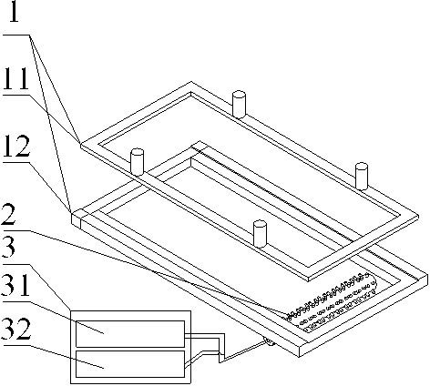
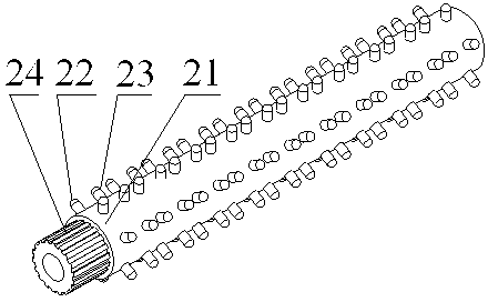
[0039] Such as Figure 1 to Figure 5 As shown, a detection device for LED chips and devices includes a square frame-shaped blue film or device substrate clamping fixture 1, a rotatable annular array test electrode roller 2 located under the blue film or device substrate clamping fixture 1 . Power supply and electrical parameter acquisition system 3, the annular array test electrode roller 2 includes a hollow cylindrical base 21 made of engineering plastics or bakelite, and the sides of the hollow cylindrical base 21 are evenly arranged in the axial and circumferential directions There are annular array through holes, and each annular array through hole is provided with an elastically stretchable metal test electrode extending outward. The metal test electrode includes a positive metal test electrode 22 and a negative metal test electrode 23. Each row of ring-shaped array through holes arranged in the axial direction of the hollow cylindrical base 21 is evenly spaced, and each ...

Embodiment 2

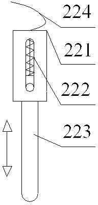
[0047] This implementation is different from Embodiment 1 in that the metal test electrode casing 221 is fixed on the hollow cylindrical base 21 in a threaded connection, and the threads are located on the outer surface of the metal test electrode sleeve 221 and in the annular array through holes of the hollow cylindrical base 21 On the surface, the protruding length of the metal test electrode can be adjusted by the number of turns of the screw thread, and this embodiment does not use an adjustment core.

Embodiment 3

[0049] The difference between this embodiment and Embodiment 1 is that the diameter of the inserted electrode length adjustment core 4 is 2 mm, the length of the test metal electrode protruding from the annular array test electrode roller 2 is 1 mm, the diameter of the probe needle 223 is 0.2 mm, and the tip distance 0.5 mm, and the distance between the positive metal test electrode 22 and the negative metal test electrode 23 is 2 mm, which is consistent with the distance between the positive and negative electrodes of a single LED device 51 to be tested. There are altogether 20 pairs of positive metal test electrodes 22 and negative metal test electrodes 23 in each row, and 12 pairs in total are evenly distributed around the annular array test electrode roller 2 . This embodiment is more suitable for applications where the size of the device is small and the arrangement density of the devices on the LED substrate is relatively high.


PUM


Abstract

The invention discloses a detection device and method for a LED chip and a device. The device comprises a blue film or a device substrate clamping jig, an annular array testing electrode, and a power supply and electrical parameter acquisition system. The annular array testing electrode is roller-shaped in appearance and provided with multiple groups of positive and negative test probes. When detection is carried out, the detection device is driven through a synchronous pulley to enable the positive and negative test probes to be exactly contacted with a positive electrode and a negative electrode of an LED chip to be tested or exactly contacted with a positive electrode and a negative electrode of a device, sweep currents are connected into a list of probes contacted with a substrate right now through a power supply in sequence, electrical parameters of the device are collected at the same time, and the synchronous pulley drives the device to roll to the next adjacent list of probes after collection is completed, and the next list of LED chips or devices are tested. The technical method is extremely high in efficiency, detection efficiency can be improved by 6-10 times compared with a traditional detection method, the detection device is applied to the LED industry, detection efficiency of LED products is greatly improved, equipment loss is reduced, product cost competitive advantages are promoted, and the detection device has good industrialization application prospects.

Description

[0001] technical field [0002] The field of the invention belongs to the field of semiconductor testing, and in particular relates to a device and method for testing LED chips and devices. Background technique [0003] LED light source has become the fourth-generation light source due to its high light efficiency, energy saving, environmental protection, long life, short response time and many other advantages. It has gradually begun to replace traditional light sources and has shown broad potential in the market. In particular, high-power LED light sources are used in a huge amount in the field of lighting. Driven by the continuous emergence of emerging application markets, the scale of the LED market has increased rapidly in recent years. The demand for LEDs in the market has risen sharply, and the demand for the matching LED production equipment has also increased rapidly. According to the data of the market research organization DisplaySearch, the market demand for LED...

Claims


Application Information

Patent Timeline
Patent Type & Authority Applications(China)
IPC IPC(8): G01R31/26
Inventor 余彬海汤勇丁鑫锐李宇吉朱本明李宗涛
Owner SOUTH CHINA UNIV OF TECH
Why Eureka
Try Eureka