Integrated circuit with memory cells comprising addressing bit lines and adjacent bit lines, and operation method
A technology of integrated circuits and memory, applied in the field of memory, can solve the problems of wrong programming adjacent bit read interference effect and so on
- Summary
- Abstract
- Description
- Claims
- Application Information
AI Technical Summary
Problems solved by technology
Method used
Image

Examples
Embodiment Construction
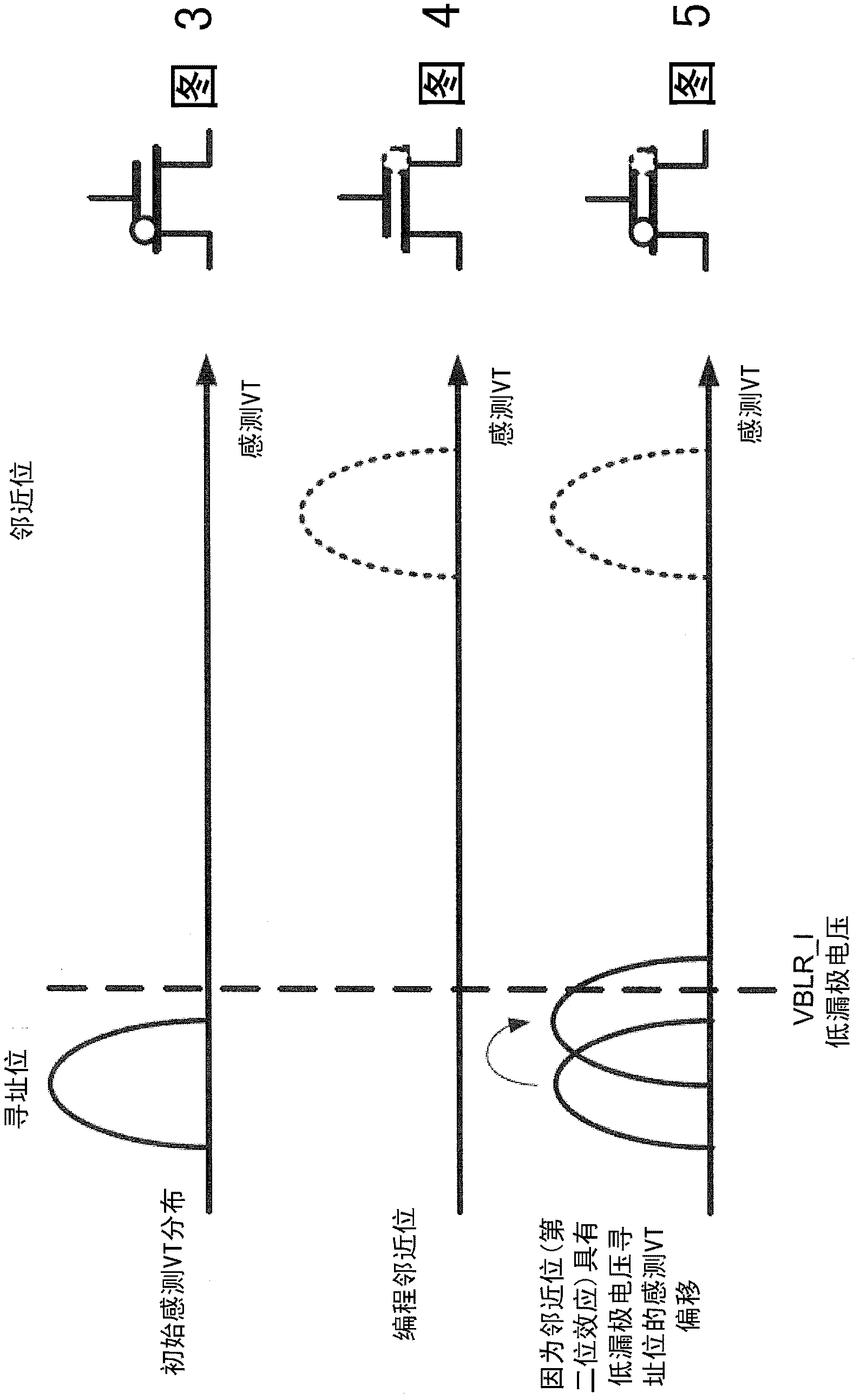
[0049] The example shown here has four possible data values in a memory cell. Other examples could be to have two possible data values, to have eight possible data values, or to have other numbers of possible data values.
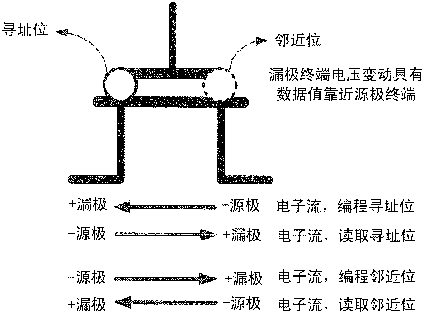
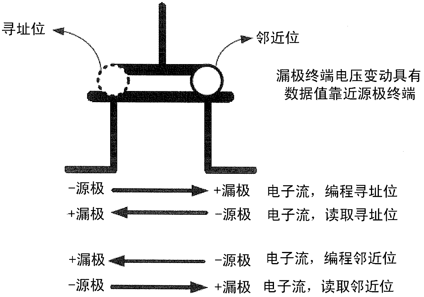
[0050] Figure 1 to Figure 2 A schematic diagram of a non-volatile memory cell, which has an address bit and adjacent bits for storing data respectively.
[0051] figure 1 A non-volatile memory cell is shown with data stored in different portions of the silicon nitride storage layer. These different portions of the same memory cell are referred to herein as "addressed bits" and "neighboring bits." In this description, the word "bit" refers to different physical locations in the charge storage layer that can store 1, 2, 3 or more bits of data. The memory cell has a gate terminal, two current carrying terminals - a drain terminal and a source terminal. The drain terminal voltage varies according to the data value near the source terminal. Because the ...
PUM
 Abstract
Description
Claims
Application Information