Organic light emitting diode (OLED) device and manufacturing method and display device thereof

A manufacturing method and device technology, which are applied in semiconductor/solid-state device manufacturing, electric solid-state devices, semiconductor devices, etc., can solve the problems of relatively high manufacturing process accuracy requirements, cumbersome and complicated manufacturing processes, and increase product production costs. The effect of reducing production costs, simplifying production processes and improving quality

Inactive Publication Date: 2013-09-25
BOE TECH GRP CO LTD
View PDF6 Cites 20 Cited by
  • Summary
  • Abstract
  • Description
  • Claims
  • Application Information

AI Technical Summary

Problems solved by technology

The organic light-emitting layer 105' usually includes three colors of organic light-emitting materials: red, green, and blue. A hole-blocking layer 12' is formed between the organic light-emitting layer 105' and the electron-transporting layer 1042' formed by organic light-emitting materials of three colors of blue, but its disadvantage is that OLED devices with such a structure need to be patterned many times. The organic light-emitting layer 105' and the hole blocking layer 12' having three colors of red, green, and blue are respectively formed by the process. In this way, not only the manufacturing process is relatively cumbersome and complicated, but also the requirements for the manufacturing process precision are relatively high, so that Seriously restrict the finished product rate of the product and increase the production cost of the product

Method used


Image

  • Organic light emitting diode (OLED) device and manufacturing method and display device thereof
  • Organic light emitting diode (OLED) device and manufacturing method and display device thereof
  • Organic light emitting diode (OLED) device and manufacturing method and display device thereof

Examples


Embodiment Construction

[0022] The following will clearly and completely describe the technical solutions in the embodiments of the present invention with reference to the accompanying drawings in the embodiments of the present invention. Obviously, the described embodiments are only some, not all, embodiments of the present invention. Based on the embodiments of the present invention, all other embodiments obtained by persons of ordinary skill in the art without making creative efforts belong to the protection scope of the present invention.

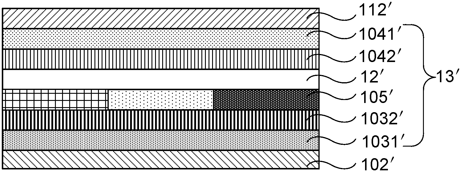
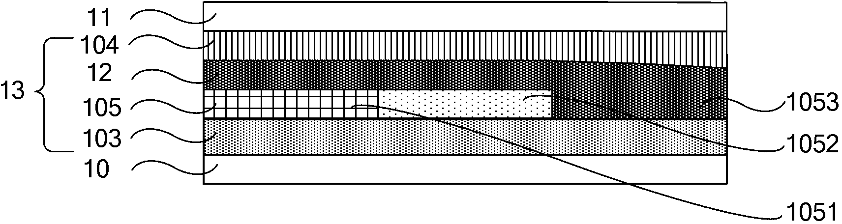
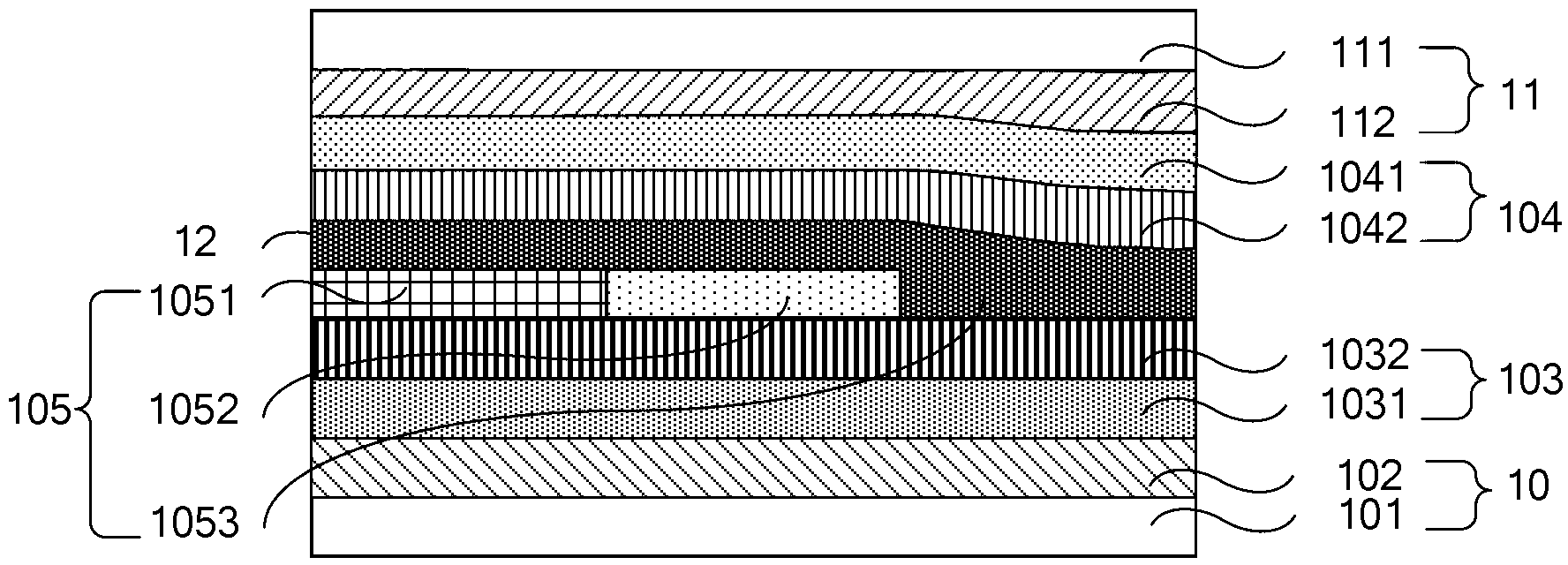
[0023] The invention provides an OLED device, such as figure 2 shown, including:

[0024] The first electrode 10, the second electrode 11 and the organic thin film layer 13 between the first electrode 10 and the second electrode 11, the organic thin film layer 13 includes a hole layer 103, an electron layer 104, and a hole layer 103 and an electron layer. The organic light-emitting layer 105 between the layers 104; in addition, the organic thin film layer 13...


PUM


Abstract

The invention discloses an organic light emitting diode (OLED) device and a manufacturing method and a display device thereof, relating to the technical field of display. The production process of the OLED device can be simplified, the production cost is reduced, and the product quality is improved. The OLED device comprises a first electrode, a second electrode and an organic film layer, wherein the organic film layer comprises a hole layer, an electronic layer and an organic luminous layer positioned between the hole layer and the electronic layer; the organic film layer also comprises a hole barrier layer; the organic luminous layer comprises a first luminous unit, a second luminous unit and a third luminous unit; the hole barrier layer and the third luminous unit are formed through a one-step composition process. The OLED device is suitable for manufacturing a display panel.

Description

technical field [0001] The invention relates to the field of display technology, in particular to an OLED device, a manufacturing method thereof, and a display device. Background technique [0002] OLED (Organic Light Emitting Diode, Organic Light Emitting Diode) display is a self-luminous display. Compared with LCD (liquid crystal display, liquid crystal display), OLED display does not require a backlight source, so OLED display is thinner and lighter. In addition, OLED display also It has the advantages of high brightness, low power consumption, wide viewing angle, high response speed, and wide operating temperature range, and is increasingly used in various high-performance display fields. [0003] The light-emitting mechanism of OLED is that under the action of an external electric field, electrons and holes are respectively injected into the organic light-emitting material from the positive and negative poles, thereby migrating, recombining and decaying in the organic l...

Claims


Application Information

Patent Timeline
Patent Type & Authority Applications(China)
IPC IPC(8): H01L51/50H01L51/52H01L51/54H01L51/56H01L27/32
CPCY02E10/549Y02P70/50H10K59/35H10K85/623H10K85/615H10K85/622H10K85/626H10K85/326H10K85/324H10K85/342H10K77/111H10K50/125H10K50/18
Inventor 李娜李周炫皇甫鲁江
Owner BOE TECH GRP CO LTD
Why Eureka
Try Eureka