Method for manufacturing photovoltaic solder strip

A technology for photovoltaic ribbons and production methods, applied in welding media, welding equipment, welding/cutting media/materials, etc., can solve the problems of high processing and production costs, improve production efficiency, have a wide range of coating thicknesses, and increase optical utilization Effect

Inactive Publication Date: 2013-10-09
TRINA SOLAR CO LTD
View PDF7 Cites 16 Cited by
  • Summary
  • Abstract
  • Description
  • Claims
  • Application Information

AI Technical Summary

Problems solved by technology

However, the processing and production cost of this kind of welding strip is relatively high now, how to reduce the processing and production cost of welding strip to realize industrial application is the focus of current research

Method used


Image

  • Method for manufacturing photovoltaic solder strip
  • Method for manufacturing photovoltaic solder strip

Examples


Embodiment 1

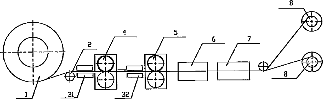
[0024] Such as figure 1 Shown, a kind of production method of photovoltaic ribbon, the process step of this method is as follows:

[0025] a) The raw copper strip 2 is unwound at a constant speed through the master material unwinding 1, and is transferred to the embossing device 4 through the first positioning guide device 31, and the raw copper strip 2 is embossed through the embossing device 4, so that the copper forming a structure with reflective grooves on the surface of belt 2 to obtain the first semi-finished product;

[0026] b) It is then transferred to the cutting device 5 by the second positioning guide device 32, and the first semi-finished product is cut into multiple copper strips with required width by the cutting device 5;

[0027] c) The slit copper strip is annealed through the annealing device 6 to form a second semi-finished product;

[0028] d) Then the second semi-finished product enters the electroplating device 7, reasonably selects the coating metal,...

Embodiment 2

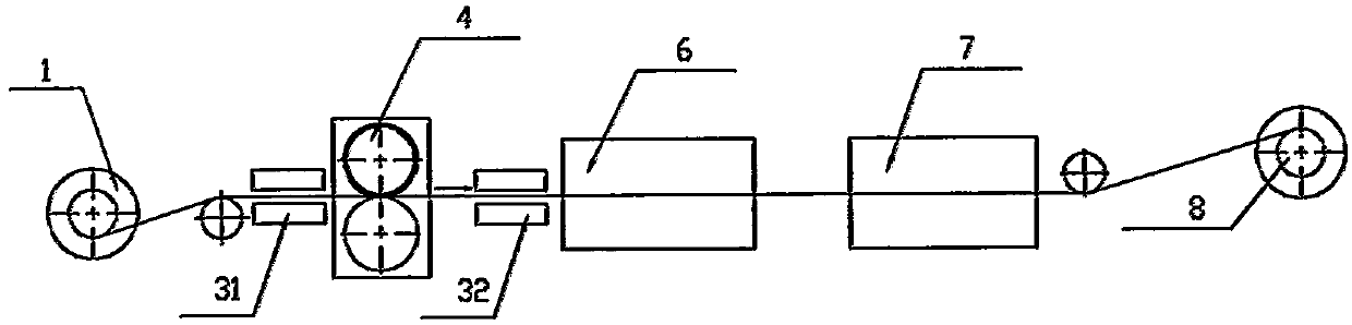
[0031] Such as figure 2 Shown, a kind of production method of photovoltaic ribbon, the process step of this method is as follows:

[0032] a) The raw copper strip with the required width is transferred to the embossing device 4 through the first positioning and guiding device 31, and the raw copper strip is embossed through the embossing device 4 to form reflective grooves on the surface of the copper strip structure to obtain the first semi-finished product;

[0033] b) then transported by the second positioning guide device 32 to the annealing device 6 for annealing treatment to form a second semi-finished product;

[0034] c) Then the second semi-finished product enters the electroplating device 7, reasonably selects the coating metal, and controls the thickness of the coating to be 1 μm to 30 μm, and performs electroplating treatment on the second semi-finished product to obtain the required photovoltaic ribbon;

[0035] d) Finally, the obtained photovoltaic ribbon is r...


PUM

PropertyMeasurementUnit
thicknessaaaaaaaaaa
thicknessaaaaaaaaaa
thicknessaaaaaaaaaa

Abstract

The invention discloses a method for manufacturing a photovoltaic solder strip. The method for manufacturing the photovoltaic solder strip includes the flowing steps: a, embossing a raw material, namely a copper strip, with a metal embossing process, forming a reflective groove structure on the surface of the copper strip, obtaining a first semi-finished product, b, conducting an annealing treatment on the first semi-finished product with an annealing process, forming a second semi-finished product, c, selecting proper coated metal, conducting electroplating on the second semi-finished product with an electroplating process, controlling the plating thickness and making the plating thickness to be ranged from 1 micrometer to 30 micrometers, and obtaining the needed photovoltaic solder strip. By means of the photovoltaic solder strip manufactured through the above method, the optical use ratio of a solar cell module can be improved, the manufacturing cost of the photovoltaic solder strip is reduced, the work efficiency of the photovoltaic solder strip is improved, and industrialized production is achieved.

Description

technical field [0001] The invention relates to a production method of a photovoltaic welding ribbon, which belongs to the technical field of solar cell equipment. Background technique [0002] At present, the photovoltaic ribbon is the key auxiliary material for connecting solar cells into strings in the solar module system. After the solar cells are connected by the ribbon, a complete electrical path is formed. The light energy is converted into electrical energy by the solar cell, and the generated current is formed by the ribbon. The transmission circuit provides the access basis for utilizing solar energy. The surface of ordinary ribbon is relatively flat after welding, and the light entering the component is incident on the flat ribbon surface, which cannot be used through mirror reflection. There are some special shaped ribbons in the prior art, and the surface is processed into certain reflective grooves. structure, the light incident on the groove structure is refl...

Claims


Application Information

Patent Timeline
Patent Type & Authority Applications(China)
IPC IPC(8): B23K35/40
Inventor 陈辉张舒杨泽民
Owner TRINA SOLAR CO LTD
Why Eureka
Try Eureka