Factory acceptance test system and method for wafer

A wafer acceptance test and measurement technology, applied in the field of wafer acceptance test system, can solve the problems of low test efficiency and cost reduction, and achieve the effect of reducing cost and improving test efficiency

Active Publication Date: 2013-10-09
SHANGHAI HUALI MICROELECTRONICS CORP
View PDF7 Cites 6 Cited by
  • Summary
  • Abstract
  • Description
  • Claims
  • Application Information

AI Technical Summary

Problems solved by technology

[0011] In view of the above existing problems, the present invention provides a wafer acceptance test system and method to overcome the problem in the prior art that the wafer needs to be retested due to charge accumulation, thereby reducing the test efficiency, and also overcomes the problem of Excessive accumulated charge will cause damage to the device, improve test efficiency, will not affect the shipment schedule at the end of the month, and reduce the cost of the product

Method used


Image

  • Factory acceptance test system and method for wafer
  • Factory acceptance test system and method for wafer
  • Factory acceptance test system and method for wafer

Examples


Embodiment 1

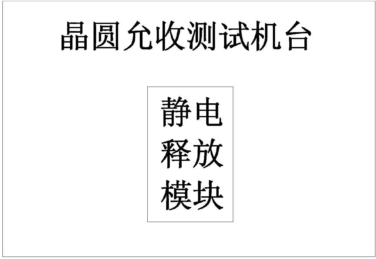
[0040] image 3 It is a schematic structural diagram of the wafer acceptance test system provided in Embodiment 1 of the present invention; as shown in the figure, the wafer acceptance test system includes a wafer acceptance test machine and an electrostatic discharge module, and the electrostatic discharge module is located on the wafer On the acceptance test machine to perform electrostatic discharge operation on the wafer acceptance test machine. Wherein, the electrostatic discharge module includes a ground contact pad. When all pins on the wafer acceptance test machine are electrically connected to the ground contact pad, the electrostatic discharge module performs electrostatic discharge operation on the wafer acceptance test machine. At this time , the voltage on the ground contact pad is 0V.

[0041]At the same time, the grounding contact pad is a grounding module of the wafer acceptance testing machine; or the grounding contact pad is a measurement module of the wafer...

Embodiment 2

[0045] Figure 4 It is a schematic flow chart of the wafer acceptance test method provided by Embodiment 2 of the present invention; as shown in the figure, before performing the wafer acceptance test process on the wafer, first perform an electrostatic discharge operation, and the All pins in the platform are connected to the measurement module in the wafer acceptance tester, and a 0V voltage is applied to the high-power power supply in the wafer acceptance tester, and the high-power power supply is electrically connected to the measurement module so that The voltage on the measurement module is 0V, after the electrostatic discharge operation lasts for 0.03s~0.3s, such as 0.03s, 0.13s, 0.19s, 0.23s, 0.29s, 0.3s, etc., disconnect the pins from the measurement module connection, thus completing the electrostatic discharge operation;

[0046] Then use the wafer acceptance test machine to perform the wafer acceptance test process on the wafer;

[0047] Finally, carry out the el...


PUM


Abstract

The invention discloses a factory acceptance test system and method for a wafer. The factory acceptance test method for the wafer can add at least electrostatic discharge operation before factory acceptance test process for the wafer and can further add at lest at least electrostatic discharge operation after the factory acceptance test process for the wafer, so that when the factory acceptance test process for the wafer is carried out, static electricity in a factory acceptance test machine for the wafer is discharged. Thus, the problems, caused by charge accumulation, of repeatedly testing the wafer and reducing the test efficiency in the prior art are solved, the problem of component damage caused by too many accumulated charges is further solved, the test efficiency is improved, delivery schedule at the end of a month cannot be affected, and product cost is further reduced.

Description

technical field [0001] The invention relates to the technical field of semiconductor testing, in particular to a wafer acceptance testing system and method. Background technique [0002] The manufacturing process of integrated circuit chips is a process that requires precise control, and a small omission will cause a large number of products to be scrapped. WAT (Wafer Acceptance Test, Wafer Acceptance Test) is an important measurement site in the chip manufacturing process. The basic principle is to test the test key located in the dicing lane on the wafer, and the results of the key parameters tested show whether the electrical performance of the chip on the wafer meets the customer's requirements. [0003] The characteristics of the foundry determine the complex product mix. The requirements for WAT are large amount of test data, accurate test data and fast test speed. WAT testing problems will waste its production capacity, and in severe cases will cause wafer (wafer) ...

Claims


Application Information

Patent Timeline
Patent Type & Authority Applications(China)
IPC IPC(8): G01R31/26
Inventor 沈茜周波
Owner SHANGHAI HUALI MICROELECTRONICS CORP
Why Eureka
Try Eureka