Epitaxial wafer of light emitting diode
A technology of light-emitting diodes and epitaxial wafers, applied in the field of epitaxial wafers, can solve the problems that the InGaN layer cannot effectively release stress, affect the quality of epitaxial wafers and luminous efficiency, and achieve the effect of improving luminous efficiency
- Summary
- Abstract
- Description
- Claims
- Application Information
AI Technical Summary
Problems solved by technology
Method used
Image

Examples
Embodiment
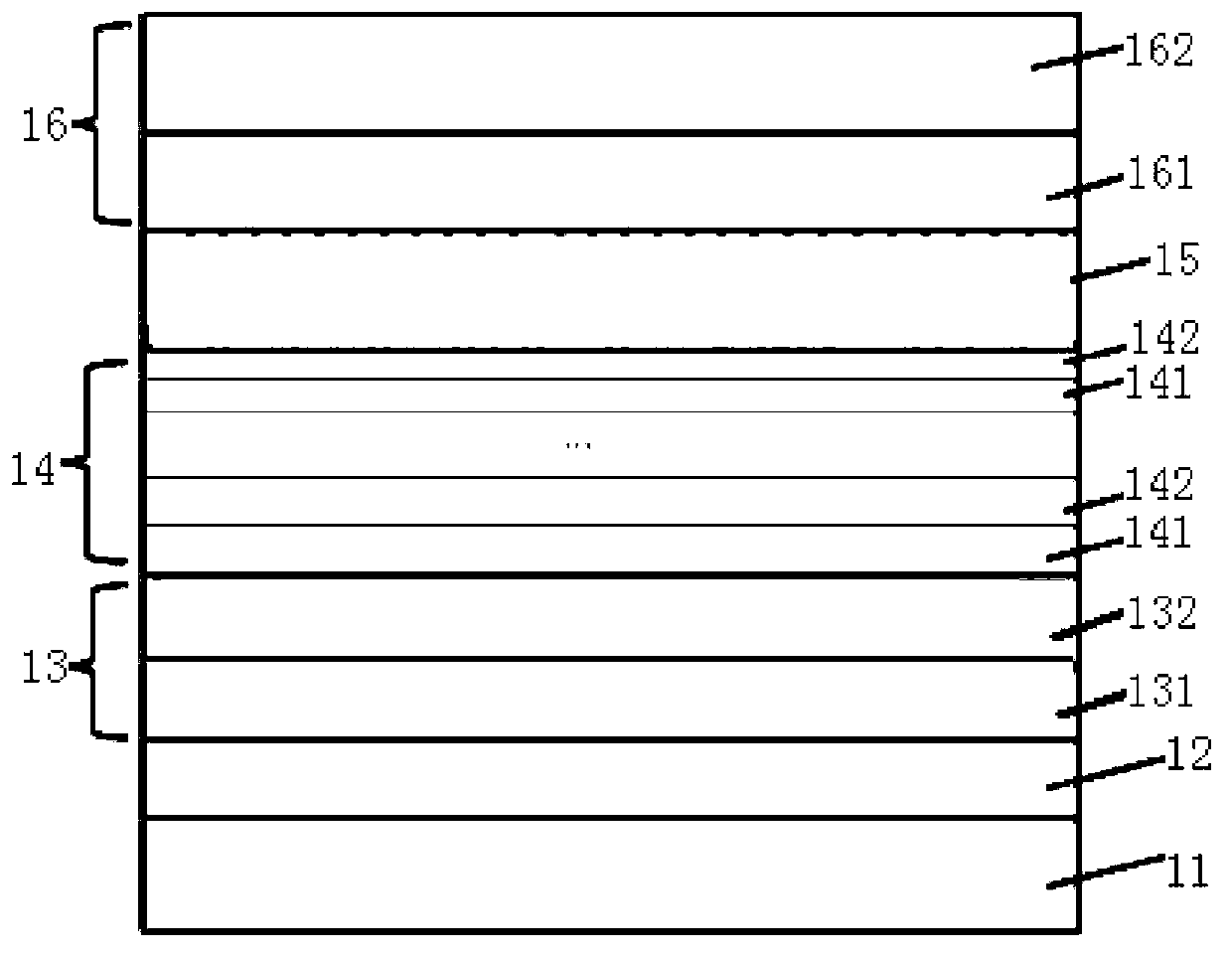
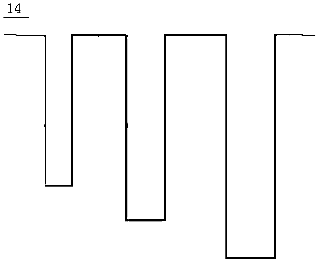
[0031] An embodiment of the present invention provides an epitaxial wafer of a light emitting diode, such as figure 1 As shown, the epitaxial wafer includes: a substrate 11, and a buffer layer 12, an n-type layer 13, a stress release layer, a multi-quantum well layer 15 and a p-type layer 16 stacked sequentially on the substrate 11, and the stress release layer 14 is Multi-cycle structure, each cycle includes In x Ga 1-x N layer 141 and grown on In x Ga 1-x The GaN layer 142 on the N layer 141, the In in each periodic structure of the stress release layer 14 x Ga 1-x The thickness of the N layer 141 increases from bottom to top, for details, see figure 2 .
[0032] It should be noted that the "bottom" in "from bottom to top" refers to the In layer in contact with the n-type layer 13. x Ga 1-x N layer, "upper" refers to the In that is closest to the multi-quantum well layer 15 x Ga 1-x N layers.
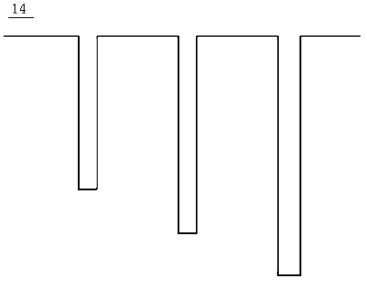
[0033] Preferably, as image 3 As shown in the conduction band schem...
PUM
 Abstract
Description
Claims
Application Information
 - Generate Ideas
- Intellectual Property
- Life Sciences
- Materials
- Tech Scout
- Unparalleled Data Quality
- Higher Quality Content
- 60% Fewer Hallucinations
Browse by: Latest US Patents, China's latest patents, Technical Efficacy Thesaurus, Application Domain, Technology Topic, Popular Technical Reports.
© 2025 PatSnap. All rights reserved.Legal|Privacy policy|Modern Slavery Act Transparency Statement|Sitemap|About US| Contact US: help@patsnap.com