Power factor compensating device
A power factor compensation and pin technology, applied in the field of switching power supply, can solve the problems of reducing the utilization rate of power generation equipment, increasing reactive power, etc., to achieve the effect of improving conduction angle, improving power factor, and reducing pollution
- Summary
- Abstract
- Description
- Claims
- Application Information
AI Technical Summary
Problems solved by technology
Method used
Image
Examples
Embodiment Construction
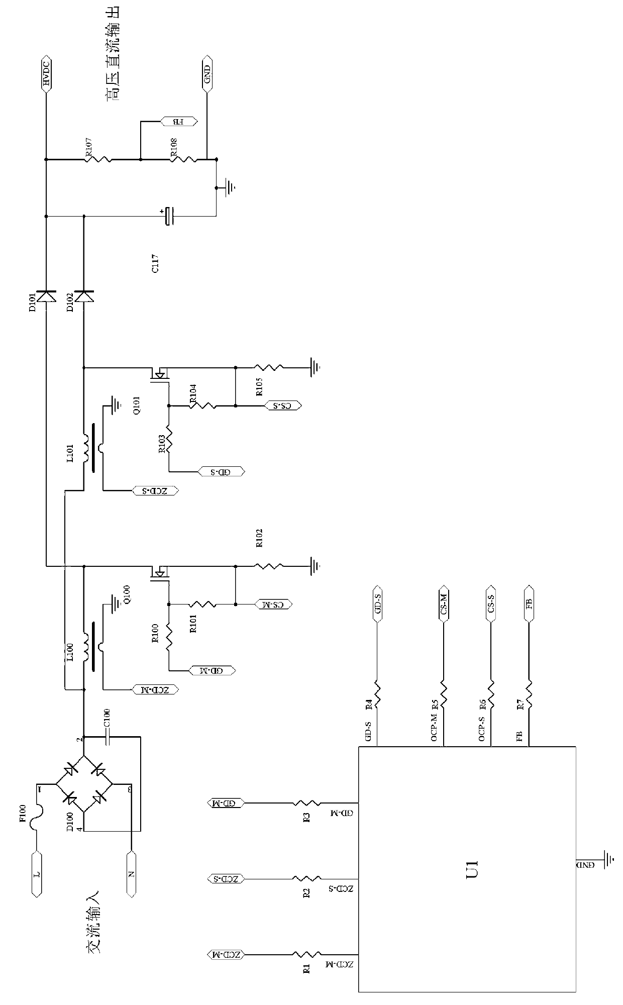
[0012] Such as figure 1 The shown power factor compensation device adopts BOOST boost circuit, which specifically includes a soft switching cycle module, a parallel interleaved module, a magnetic integration module, a current feedback detection module and a voltage feedback detection module, and the pin GD- of the soft switching cycle module M, MOSFETQ100, inductor L100, and pin ZCD-M are connected, and pin GD-S, MOSFETQ101, inductor L101, and pin ZCD-S are connected. U1 is the control chip. The pin GD-M of the control chip U1 first generates a driving signal to turn on the MOSFETQ100. At this time, the current of the inductor L100 starts to rise. When the driving signal generated by the pin GD-M ends, the MOSFETQ100 is cut off. When the current of the inductor L100 starts to drop, the pin ZCD-M of the control chip U1 detects that the inductor current drops to zero through the auxiliary winding of the inductor L100, and the pin GD-M of the control chip U1 generates a driving s...
PUM
 Abstract
Description
Claims
Application Information
