Reusable logical gate of mixed structure of MOS transistor and single-electron transistor

A single-electron transistor, multiplexing logic technology, applied in the direction of logic circuits with logic functions, etc., can solve the problem of difficult to meet circuit power consumption, integration, reliability, difficult MOS tubes to reduce the use of MOS tubes, and poor logic circuit programmability. and other problems, to achieve the effect of simple structure, reduced number of devices, and high integration

Active Publication Date: 2013-10-09
FUZHOU UNIV
View PDF2 Cites 9 Cited by
  • Summary
  • Abstract
  • Description
  • Claims
  • Application Information

AI Technical Summary

Problems solved by technology

Due to the limitations of MOS tube functions, it is difficult to greatly reduce the use of MOS tubes by optimizing the performance of MOS tubes
In addition, logic circuits based on MOS tubes have poor programmability, and it is difficult to convert between different logic gates
Therefore, the design method based on MOS transistors is difficult to meet the requirements of the new generation of circuits in terms of power consumption, integration, reliability, etc.

Method used


Image

  • Reusable logical gate of mixed structure of MOS transistor and single-electron transistor
  • Reusable logical gate of mixed structure of MOS transistor and single-electron transistor
  • Reusable logical gate of mixed structure of MOS transistor and single-electron transistor

Examples


Embodiment Construction

[0026] The present invention will be further described below in conjunction with the accompanying drawings and embodiments.

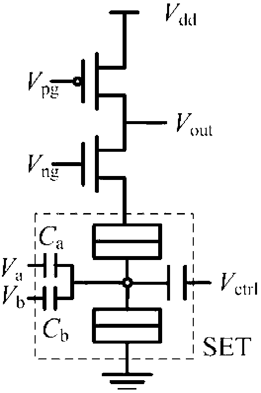
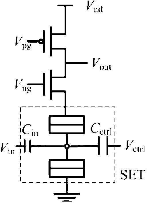
[0027] The invention designs a reusable logic gate based on the novel nanometer electronic device. This logic gate can implement all two-input logic. The novel nanoelectronic device adopted in the present invention is a single electron transistor (Single electron transistor, SET). As a typical representative of a new generation of nanoelectronic devices, SET has extremely low power consumption and ultra-small device size, and has obvious advantages over traditional microelectronic devices in terms of power consumption and working speed. Ideal device for low power consumption, high density VLSI. SET has unique Coulomb blocking and Coulomb oscillation effects, and is well compatible with MOS devices. The SET / MOS hybrid structure has the superior performance of both SET and MOS transistors, showing extremely low power consumption, ultra-small device siz...


PUM


Abstract

The invention provides a reusable logical gate based on an SET/MOS mixed structure according to a coulomb blockade oscillation effect and multiple-grid input features of the mixed structure of a single-electron transistor and an MOS transistor of a novel nano-electronical appliance. Through bias of an input end and a control end, all two-input logical functions of OR, NOR, AND, NAND, XOR and XNOR can be achieved by a logical unit without changing device parameters of a circuit, and only three PMOS transistors, three NMOS transistors and three SETs are consumed. The reusable logical gate is simple in structure, low in power consumption, high in integration level and high in reconfigurable features, and is expected to be applied to super-large-scale integration circuits with low power consumption and high integration density in future.

Description

technical field [0001] The invention relates to the technical field of integrated circuits, in particular to a reusable logic gate with a hybrid structure of MOS transistors and single electron transistors. Background technique [0002] In digital circuits, MOS transistors have binary characteristics and work in two states of on and off. The logic functions realized by using MOS transistors need to consume more devices. Due to the limitations of MOS tube functions, it is difficult to greatly reduce the use of MOS tubes by optimizing the performance of MOS tubes. In addition, logic circuits based on MOS transistors have poor programmability, and it is difficult to switch between different logic gates. Therefore, the design method based on MOS transistors is difficult to meet the requirements of the new generation of circuits in terms of power consumption, integration, and reliability. [0003] In recent years, with the introduction of new nanoelectronic devices, it has beco...

Claims


Application Information

Patent Timeline
Patent Type & Authority Applications(China)
IPC IPC(8): H03K19/20
Inventor 魏榕山陈锦锋于志敏何明华
Owner FUZHOU UNIV
Why Eureka
Try Eureka