Array substrate and display device comprising same

A technology for array substrates and display devices, applied in instruments, nonlinear optics, optics, etc., to achieve the effects of preventing light leakage, high light transmittance, and good shading effect

Active Publication Date: 2013-10-16
BOE TECH GRP CO LTD +1
View PDF5 Cites 36 Cited by
  • Summary
  • Abstract
  • Description
  • Claims
  • Application Information

AI Technical Summary

Problems solved by technology

Therefore, in order to meet the requirements of high resolution and thin, light and beautiful appeara

Method used


Image

  • Array substrate and display device comprising same
  • Array substrate and display device comprising same
  • Array substrate and display device comprising same

Examples


Embodiment 1

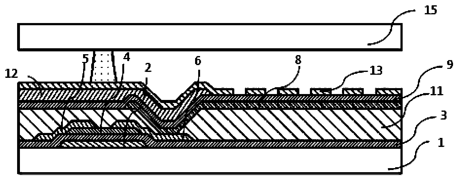
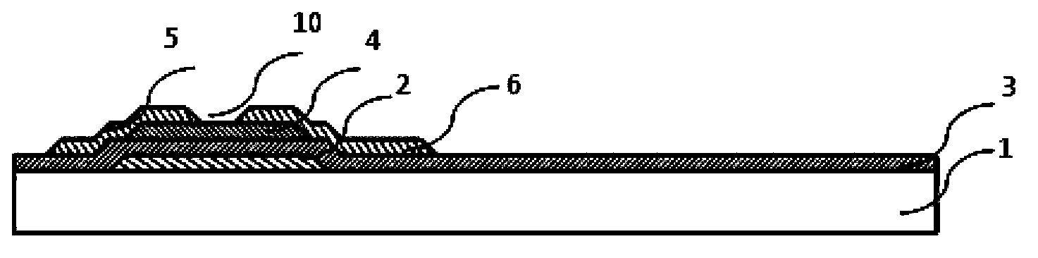
[0038] The display device of this embodiment is a liquid crystal display device. The liquid crystal display device includes an array substrate and a color filter layer formed on the array substrate, that is, the color filter layer is directly arranged on the array substrate on which the thin film transistors have been formed.

[0039] The display device of this embodiment is an ADS (ADvanced Super Dimension Switch, advanced ultra-dimensional field switching technology) mode. In this display device, the electric field generated by the edge of the slit electrode in the same plane and the slit electrode and the plate electrode The electric field generated between them forms a multi-dimensional electric field, so that all oriented liquid crystal molecules in the liquid crystal cell (between the array substrate and the packaging substrate) between the slit electrodes and directly above the electrodes can rotate, thereby improving the working efficiency of the liquid crystal and incr...

Embodiment 2

[0082] The display device in this embodiment is a TN (Twisted Nematic, twisted nematic) mode or a VA (Vertical Alignment, vertical alignment) mode. The common point of both is that the pixel electrode and the common electrode are separately arranged on the two opposite substrates of the box The difference is that the orientation layers on the opposite two substrates of the box are provided with different orientation angles, so that: in the display device of TN mode, the liquid crystal molecules are horizontally aligned; in the display device of VA mode, the liquid crystal molecules for vertical orientation.

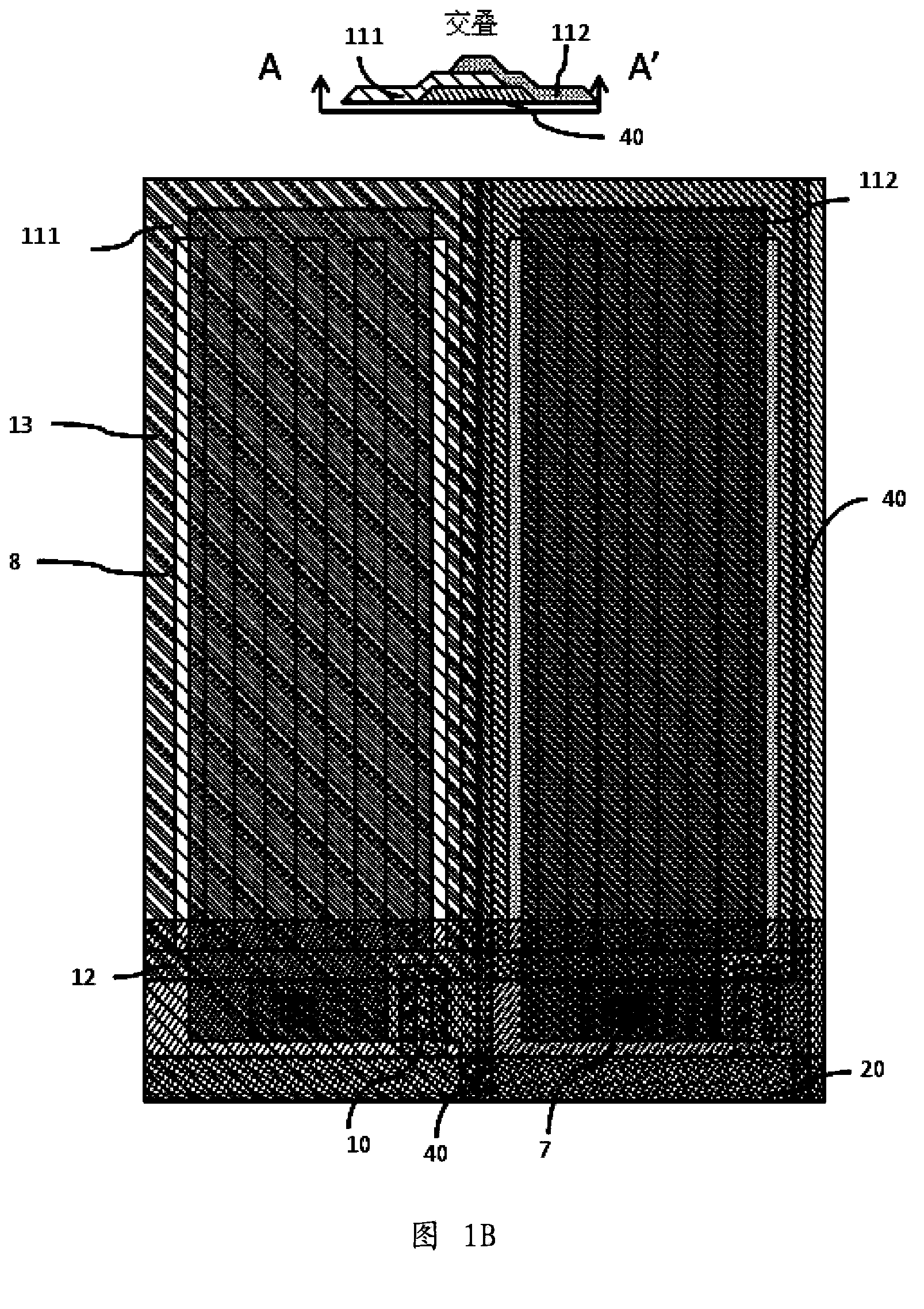
[0083] In this embodiment, the array substrate includes a substrate and a plurality of data lines and a plurality of gate lines intersecting on the substrate. The data lines and gate lines divide the substrate into a plurality of pixel areas, and the pixel areas are provided with thin film transistors, color The film layer and the black matrix, the thin film transistor in...

Embodiment 3

[0091] The display device in this embodiment is a WOLED display device, and the display device further includes a white organic electroluminescent diode.

[0092] In this embodiment, the array substrate includes a substrate and a plurality of data lines and a plurality of gate lines intersecting on the substrate. The data lines and gate lines divide the substrate into a plurality of pixel areas, and the pixel areas are provided with thin film transistors, color The film layer and the black matrix, the thin film transistor includes a gate, a source and a drain, the color filter layer is arranged directly above the source and drain of the upper layer in the thin film transistor, and the setting direction of the color filter layer is the same as the extending direction of the data line Similarly, the black matrix is ​​disposed above the color filter layer corresponding to the grid lines.

[0093] Wherein, in the thin film transistor, the gate is arranged below the source and the ...


PUM


Abstract

The invention belongs to the technical field of display, in particular to an array substrate and a display device comprising the same. The array substrate comprises a substrate as well as a plurality of data cables and a plurality of grid lines which are arranged on the substrate in a crossed manner, wherein the data cables and the grid lines divide the substrate into a plurality of pixel areas, and thin film transistors are arranged in the pixel areas; each thin film transistor comprises a grid electrode, a source electrode and a drain electrode; and the array substrate further comprises colored films and black matrixes, the colored films are directly arranged on grid electrodes located on the upper layers of the thin film transistors or above the source electrodes and the drain electrodes which are located on the upper layers of the thin film transistors, the arrangement directions of the colored films are identical with extending directions of the data cables, and the black matrixes are arranged above the grid lines corresponding to the colored films. The array substrate and the display device have benefits as follows: the aperture ratio is higher, the image picture contrast is high, the cost is lower, the preparation process is simpler, and requirements for high resolution, lightness and attractiveness are easy to meet.

Description

technical field [0001] The invention belongs to the field of display technology, and in particular relates to an array substrate and a display device including the array substrate. Background technique [0002] With the development of technology, flat panel display devices have replaced bulky CRT display devices and become the current mainstream display devices. Currently, commonly used flat panel display devices mainly include LCD (Liquid Crystal Display: liquid crystal display device) and OLED (Organic Light-Emitting Diode: organic electroluminescent diode) display device. [0003] The liquid crystal display device includes a backlight source, an array substrate and a color filter substrate for the cell, and liquid crystals are filled between the array substrate and the color filter substrate. A thin film transistor (Thin Film Transistor: TFT for short) is arranged on the array substrate, and the thin film transistor is used to control the emission of light to realize ima...

Claims


Application Information

Patent Timeline
IPC IPC(8): G02F1/1335G02F1/1343G02F1/1362G02F1/1368
CPCG02F1/134309G02F1/1362G02F1/134372G02F1/136222
Inventor 高永益黄炜赟南英瑛朴进山金楻
Owner BOE TECH GRP CO LTD
Why Eureka
Try Eureka