Unlock instant, AI-driven research and patent intelligence for your innovation.

Touch control panel and manufacturing method thereof

A technology of a touch panel and a manufacturing method is applied in the touch panel and its manufacturing field which can avoid electrostatic damage, and can solve the problems of scrapping of touch sensing units and the like

Inactive Publication Date: 2013-10-23
AU OPTRONICS CORP
View PDF5 Cites 11 Cited by
  • Summary
  • Abstract
  • Description
  • Claims
  • Application Information

AI Technical Summary

Problems solved by technology

However, after the mother board is cut, the test circuit will inevitably be exposed from the edge of the touch panel, which will make the subsequent electrostatic test (Electro Static Discharge, ESD) or product assembly, the static electricity will be exposed by the above test. The circuit enters the touch panel, causing components in the touch panel that are electrically connected to the test circuit, such as flexible circuit boards, printed circuit board assemblies or touch sensing units, to be scrapped due to electrostatic damage

Method used


Image

  • Touch control panel and manufacturing method thereof
  • Touch control panel and manufacturing method thereof
  • Touch control panel and manufacturing method thereof

Examples


Embodiment Construction

[0036] In order to make the technical content disclosed in this application more detailed and complete, reference may be made to the drawings and the following various specific embodiments of the present invention, and the same symbols in the drawings represent the same or similar components. However, those skilled in the art should understand that the examples provided below are not intended to limit the scope of the present invention. In addition, the drawings are only for schematic illustration and are not drawn according to their original scale. The specific implementation manners of various aspects of the present invention will be further described in detail below with reference to the accompanying drawings.

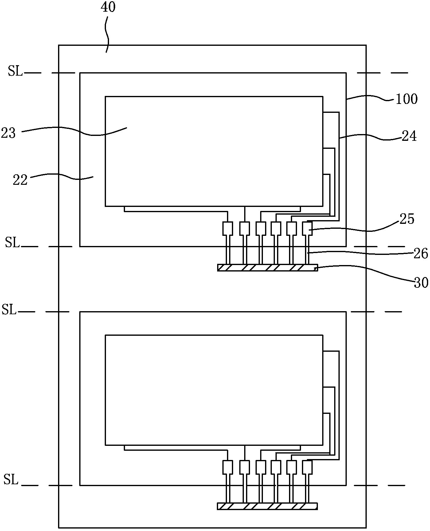
[0037] See Figure 1-Figure 6 , figure 1 Shown is a schematic diagram of the manufacturing method of the touch panel according to the present invention; figure 2 Shown is a flow chart of the steps of the manufacturing method of the touch panel according to the p...


PUM


Abstract

The invention provides a touch control panel and a manufacturing method thereof. The manufacturing method comprises the following steps: providing a mother board; forming an induction line layer in each touch control area of the mother board; forming a peripheral line layer in each peripheral area of the mother board, wherein each peripheral line layer comprises at least one connecting pad and at least one testing line, each connecting pad is electrically connected with a corresponding touch control sensing unit, and each testing line is electrically connected with a corresponding connecting pad; introducing a test signal through each testing line to test each touch control sensing unit; forming a first insulation layer in each peripheral area; patterning each first insulation layer, wherein each testing line and each corresponding connecting pad form an open circuit, and each first insulation layer comprises at least one first contact window to expose partial area of each corresponding connecting pad; cutting the mother board along a cutting line to form the touch control panel. According to the invention, static cannot enter the exposed testing lines when a touch control panel finished product is tested in the ESD (Electro Static Discharge) or is assembled for use, so that the phenomenon that a flexible circuit board, a printed circuit board assembly or the touch control sensing units are damaged and scrapped by static can be avoided.

Description

technical field [0001] The present invention relates to a touch panel and a manufacturing method thereof, and in particular to a touch panel capable of avoiding electrostatic damage and a manufacturing method thereof. Background technique [0002] As the development of electronic product design is becoming more and more user-oriented, products using touch panels have gradually become the mainstream in the market, considering the convenience of users' operation, such as smart phones or tablet computers. Therefore, touch Panels have become an important and integral part of these commodities. However, when the touch panel in the prior art is subjected to an Electro Static Discharge (ESD) test on a finished product or a semi-finished product, there is often an unavoidable problem of damage by static electricity. [0003] Generally speaking, in order to judge the yield rate in advance, the touch panel needs to be tested after the touch sensing unit is formed. The touch panel ha...

Claims


Application Information

Patent Timeline
IPC IPC(8): G06F3/041
Inventor 陈建宇莊文奇
Owner AU OPTRONICS CORP