Method for exposing through silicon via

A technology of through-silicon vias and dielectric layers, applied in electrical components, semiconductor/solid-state device manufacturing, circuits, etc., can solve the problems of shallow-dish effect, inability to expose part of the sidewalls of through-silicon vias, and disadvantages. The effect of reliable interconnection

Inactive Publication Date: 2013-10-23
NAN YA TECH
View PDF3 Cites 4 Cited by
  • Summary
  • Abstract
  • Description
  • Claims
  • Application Information

AI Technical Summary

Problems solved by technology

[0004] However, the disadvantage of the above-mentioned backgrinding or CMP process is the shallow dish effect
That is, the surface of the exposed copper metal layer 21 will be slightly sunken inward. In addition, part of the sidewall of the TSV 20 cannot be exposed, so the final TSV structure is not conducive to the three-dimensional When the chip is packaged, the interconnection in the vertical direction is realized

Method used


Image

  • Method for exposing through silicon via
  • Method for exposing through silicon via
  • Method for exposing through silicon via

Examples


Embodiment Construction

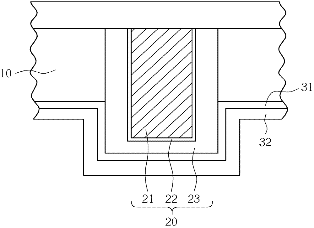
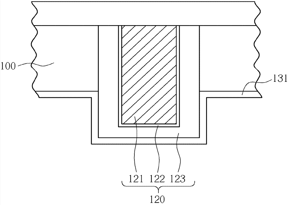
[0021] Figure 3 to Figure 7 A preferred embodiment of the present invention is illustrated. Such as image 3 As shown, firstly a TSV 120 is formed in a semiconductor substrate 100 or a silicon wafer, including a copper metal layer 121 , a barrier layer 122 and an insulating layer 123 . One end of the TSV 120 will slightly protrude from the bottom surface of the semiconductor substrate 10 or silicon wafer, such as image 3 As shown, then, a dielectric layer 131 , such as a silicon nitride layer, is covered on the bottom surface of the semiconductor substrate 10 and the TSV 120 .

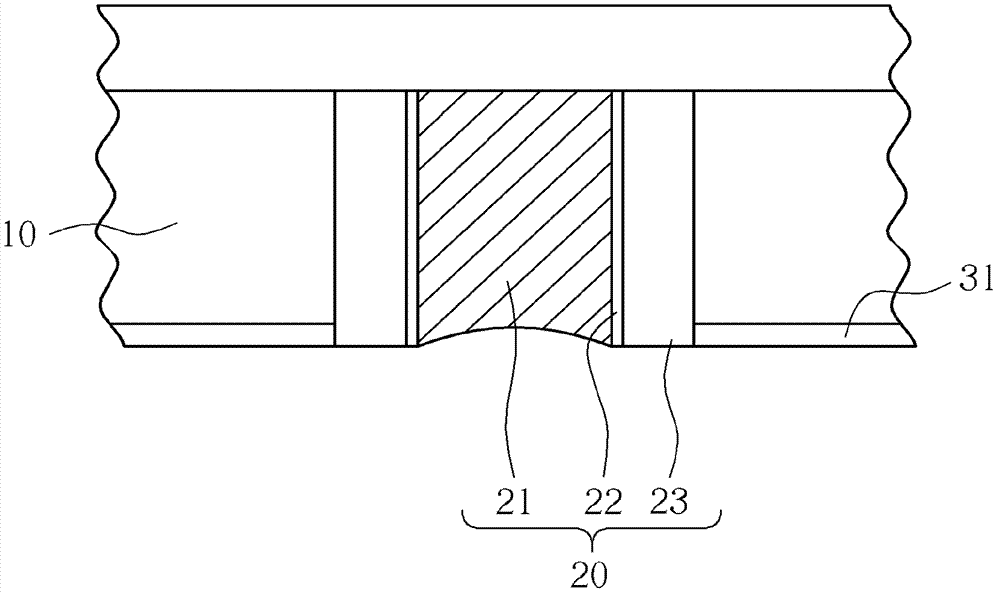
[0022] Such as Figure 4 As shown, then, a sacrificial layer 140 such as a photoresist layer is formed on the silicon nitride layer 131 . Of course, the sacrificial layer 140 can also be made of other materials, but it must be a material capable of resisting etching. Such as Figure 5 As shown, a crystal back grinding or chemical mechanical polishing (CMP) process is performed to remove part of...


PUM


Abstract

The invention discloses a method for exposing a through silicon via. The method comprises the steps of firstly forming a through silicon via in a semiconductor substrate, wherein the through silicon via comprises a copper metal layer, a barrier layer and an insulating layer; covering a dielectric layer on the bottom surface of the semiconductor substrate and the through silicon via; forming a sacrificial layer on the dielectric layer; abrading and removing a part of the sacrificial layer, the dielectric layer, the insulating layer and the barrier layer so as to expose the surface of the copper metal layer; etching a part of the insulating layer and the dielectric layer, and forming a concave region around the through silicon via; and finally removing the left sacrificial layer.

Description

technical field [0001] The present invention relates to a method for exposing a through silicon via (TSV). Background technique [0002] Through-silicon via is a conductor structure that runs through the silicon substrate. Its main function is to interconnect integrated circuit chips. Insulation layer, forming a seed layer on the insulation layer, then filling the through hole with metal by electroplating, and then exposing one end of the TSV through crystal back grinding. In this way, the size of the chip can be greatly reduced, the transistor density of the chip can be increased, the performance of electrical interconnection between layers can be improved, the operating speed of the chip can be increased, and the power consumption of the chip can be reduced. [0003] figure 1 and figure 2 One known method of exposing TSVs is illustrated. After the TSV is completed, one end of the TSV 20 will slightly protrude from the bottom surface of the semiconductor substrate 10 o...

Claims


Application Information

Patent Timeline
Patent Type & Authority Applications(China)
IPC IPC(8): H01L21/768
Inventor 陈逸男徐文吉叶绍文刘献文
Owner NAN YA TECH
Why Eureka
Try Eureka