Schottky semiconductor device with insulating layer isolated super-junction structure and preparation method for Schottky semiconductor device

A technology of semiconductor and insulating layer, applied in the field of preparation of Schottky semiconductor device with insulating layer isolation superjunction structure, can solve the problem of high voltage environment, high on-resistance and reverse leakage current that cannot be applied, and fast turn-on and turn-off speed. and other problems, to achieve the effect of improving forward conduction characteristics, increasing reverse breakdown voltage, and reducing forward conduction resistance

Inactive Publication Date: 2013-10-23
朱江
View PDF3 Cites 2 Cited by
  • Summary
  • Abstract
  • Description
  • Claims
  • Application Information

AI Technical Summary

Problems solved by technology

[0002] Power semiconductor devices are widely used in power management and power applications, especially semiconductor devices with super junction structure and Schottky structure have become an important trend in device development. Schottky devices have low forward turn-on voltage and turn-off speed At the same time, the Schottky device also has the disadvantages of large reverse leakage current and cannot be used in high-voltage environments.
[0003] Schottky diodes can be manufactured by a variety of different layout techniques. The manufacturing process of traditional trench Schottky diodes requires more masks and manufacturing steps, while traditional trench Schottky diodes have relatively High on-resistance and reverse leakage current characteristics

Method used


Image

  • Schottky semiconductor device with insulating layer isolated super-junction structure and preparation method for Schottky semiconductor device
  • Schottky semiconductor device with insulating layer isolated super-junction structure and preparation method for Schottky semiconductor device

Examples


Embodiment 1

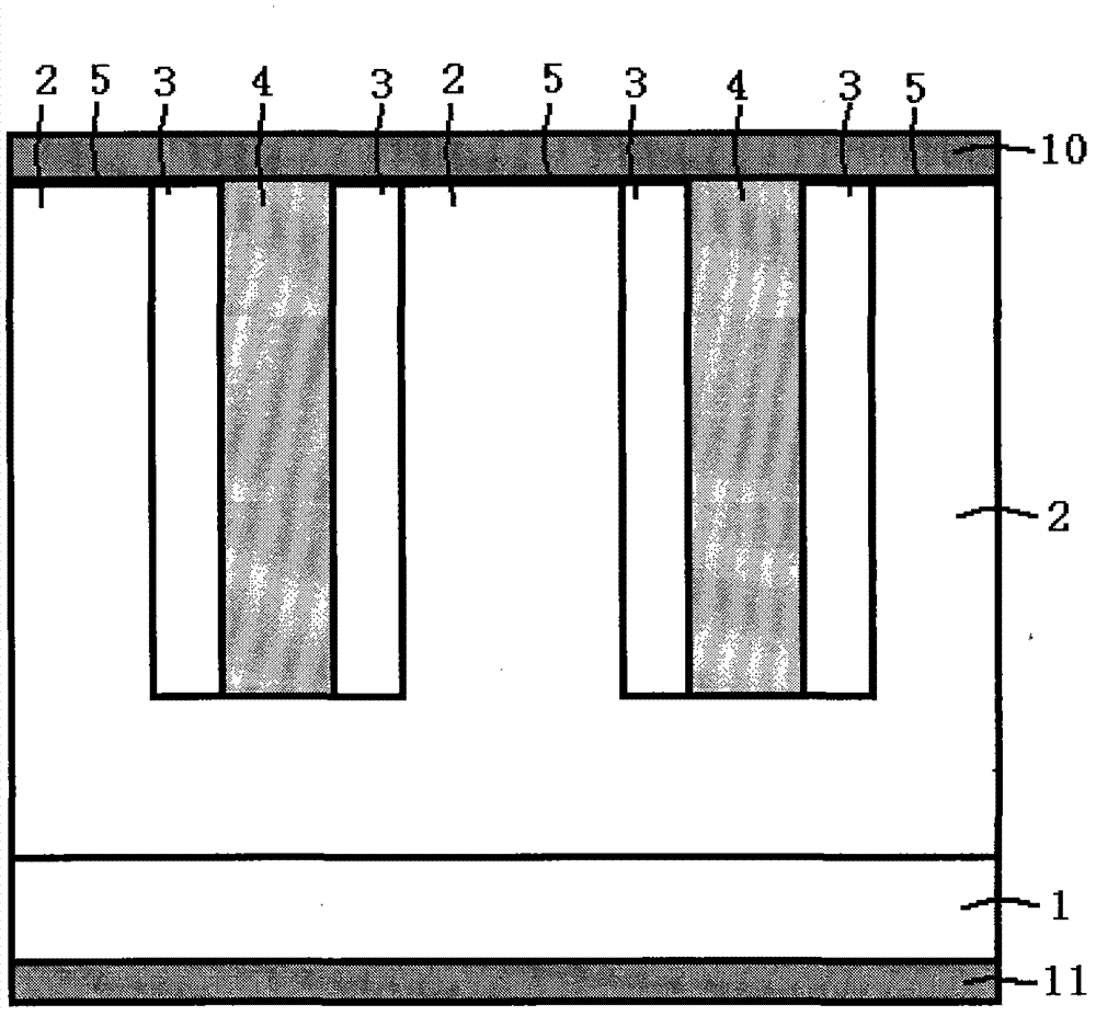
[0020] figure 1 It is a Schottky semiconductor device with insulating layer isolation super junction structure of the present invention, combined below figure 1 The semiconductor device of the present invention will be described in detail.

[0021] A Schottky semiconductor device with an insulating layer isolation superjunction structure, comprising: a substrate layer 1, which is an N conductivity type semiconductor silicon material, and the doping concentration of phosphorus atoms is 1E19 / CM 3 , on the lower surface of the substrate layer 1, the electrode is drawn out through the lower surface metal layer 11; the N-type semiconductor silicon material 2, located on the substrate layer 1, is an N-conduction type semiconductor silicon material, and the doping concentration of phosphorus atoms is 1E16 / CM 3 ; P-type semiconductor silicon material 3, located between N-type semiconductor silicon material 2 and silicon dioxide 4, is a P-type semiconductor silicon material, and the d...

Embodiment 2

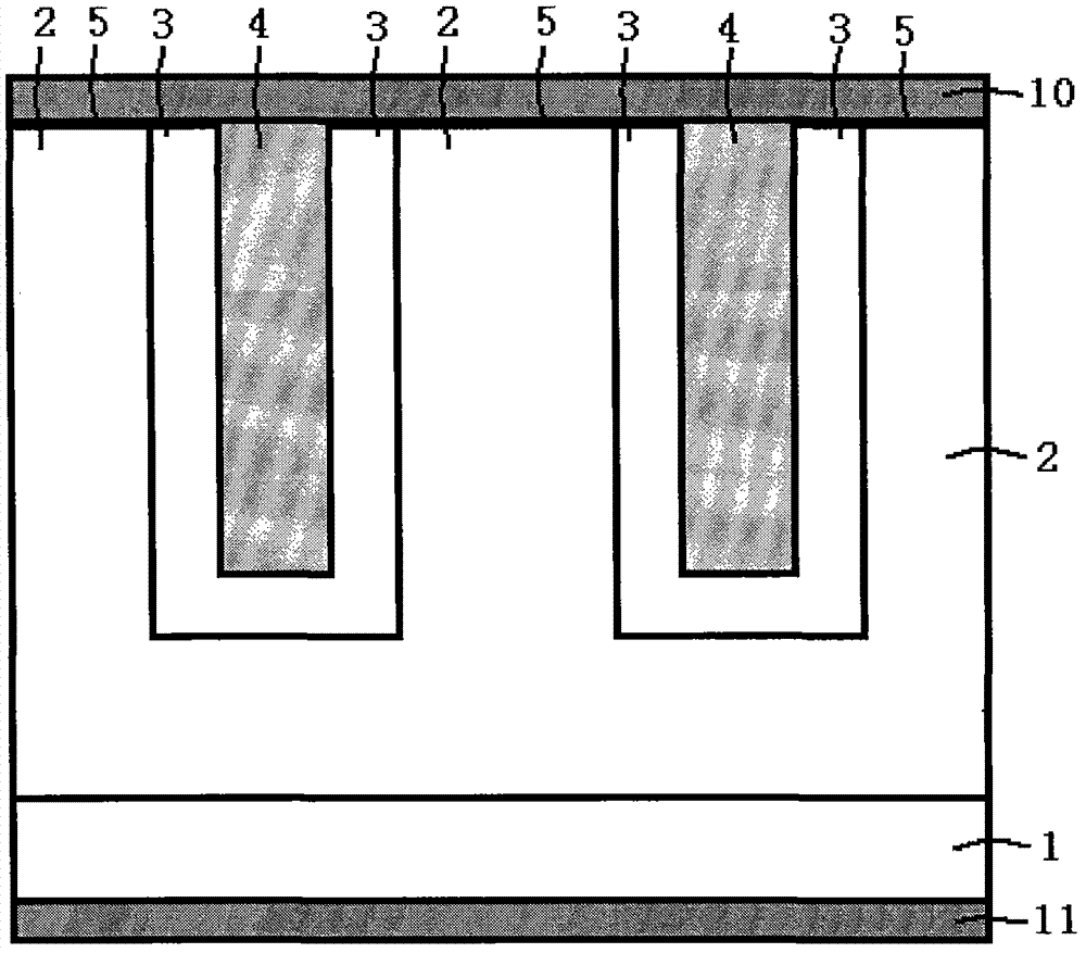
[0031] figure 2 It is a Schottky semiconductor device with insulating layer isolation super junction structure of the present invention, combined below figure 2 The semiconductor device of the present invention will be described in detail.

[0032] A Schottky semiconductor device with an insulating layer isolation superjunction structure, comprising: a substrate layer 1, which is an N conductivity type semiconductor silicon material, and the doping concentration of phosphorus atoms is 1E19 / CM 3 , on the lower surface of the substrate layer 1, the electrode is drawn out through the lower surface metal layer 11; the N-type semiconductor silicon material 2, located on the substrate layer 1, is an N-conduction type semiconductor silicon material, and the doping concentration of phosphorus atoms is 1E16 / CM 3 ; P-type semiconductor silicon material 3, located between N-type semiconductor silicon material 2 and silicon dioxide 4, is a semiconductor silicon material of P conductivi...


PUM


Abstract

The invention discloses a Schottky semiconductor device with an insulating layer isolated super-junction structure. By a groove structure, a deeper strip-shaped P-type semiconductor silicon material can be realized, when the device is connected with reverse bias, the strip-shaped P-type semiconductor silicon material and an N-type semiconductor silicon material form charge complementation to form the super-junction structure, and the electric field intensity distribution of a drift region is changed to form a flat electric field intensity distribution curve. The invention also provides a preparation method for the Schottky semiconductor device with the insulating layer isolated super-junction structure.

Description

technical field [0001] The invention relates to a Schottky semiconductor device with an insulating layer isolation super-junction structure, and also relates to a preparation method of the Schottky semiconductor device with an insulating layer isolation super-junction structure. Background technique [0002] Power semiconductor devices are widely used in power management and power applications, especially semiconductor devices with super junction structure and Schottky structure have become an important trend in device development. Schottky devices have low forward turn-on voltage and turn-off speed At the same time, the Schottky device also has the disadvantages of large reverse leakage current and cannot be used in high-voltage environments. [0003] Schottky diodes can be manufactured by a variety of different layout techniques. The manufacturing process of traditional trench Schottky diodes requires more masks and manufacturing steps, while traditional trench Schottky di...

Claims


Application Information

Patent Timeline
Patent Type & Authority Applications(China)
IPC IPC(8): H01L29/872H01L29/06H01L21/329
Inventor 朱江
Owner 朱江
Why Eureka
Try Eureka