
Network-on-chip-based optimization method for DRAM communication

An optimization method and network-on-chip technology, applied in the fields of instruments, electrical digital data processing, computers, etc., can solve problems such as performance degradation, VC number reduction, cache resource utilization reduction, etc., to achieve overall performance increase, reduce delay, improve The effect of utilization

Inactive Publication Date: 2013-11-06
XI AN JIAOTONG UNIV
View PDF3 Cites 0 Cited by
  • Summary
  • Abstract
  • Description
  • Claims
  • Application Information

AI Technical Summary

Problems solved by technology

The traditional solution is to reserve a dedicated virtual channel (VirtualChannel, VC for short) for DRAM communication, thus avoiding communication competition with nodes and improving DRAM communication performance, but this method has an obvious disadvantage : Reserving a dedicated VC may reduce the utilization of cache resources, and at the same time reduce the number of VCs available for data communication between nodes, thereby reducing the performance of the entire system

Method used


Image

  • Network-on-chip-based optimization method for DRAM communication
  • Network-on-chip-based optimization method for DRAM communication
  • Network-on-chip-based optimization method for DRAM communication

Examples


Embodiment Construction

[0019] The present invention will be further described in detail below in conjunction with the accompanying drawings.

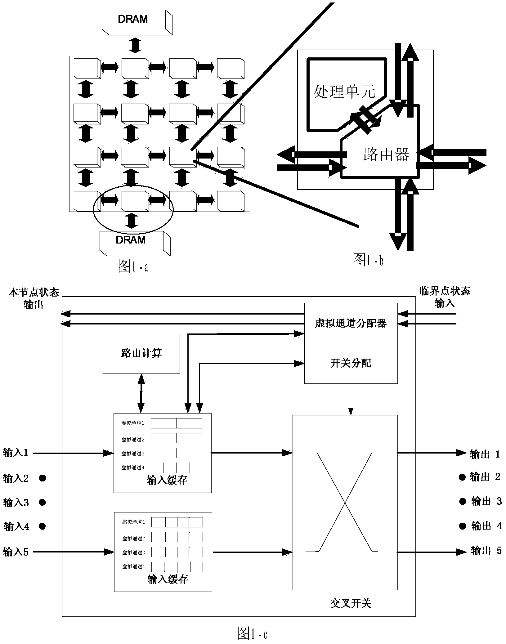
[0020] figure 1 -a is a system schematic diagram of a standard two-dimensional grid topology based on an on-chip interconnection network communication system, including a processing unit, a communication link, and a storage controller. Each square node represents a processing unit, such as CPU, DSP, etc. The double arrows indicate the communication links of the network. The oval area in the figure emphasizes the interface between the on-chip network and DRAM, which connects the on-chip network and DRAM. figure 1 -b is figure 1 - the architecture of a processing unit in a, as shown in the figure, each processing unit includes a processor and a corresponding routing unit.

[0021] figure 1 -c is a structure diagram of a standard NoC five-stage pipeline router in the prior art, specifically including: write input buffer, routing path calculation, virtual ch...


PUM


Abstract

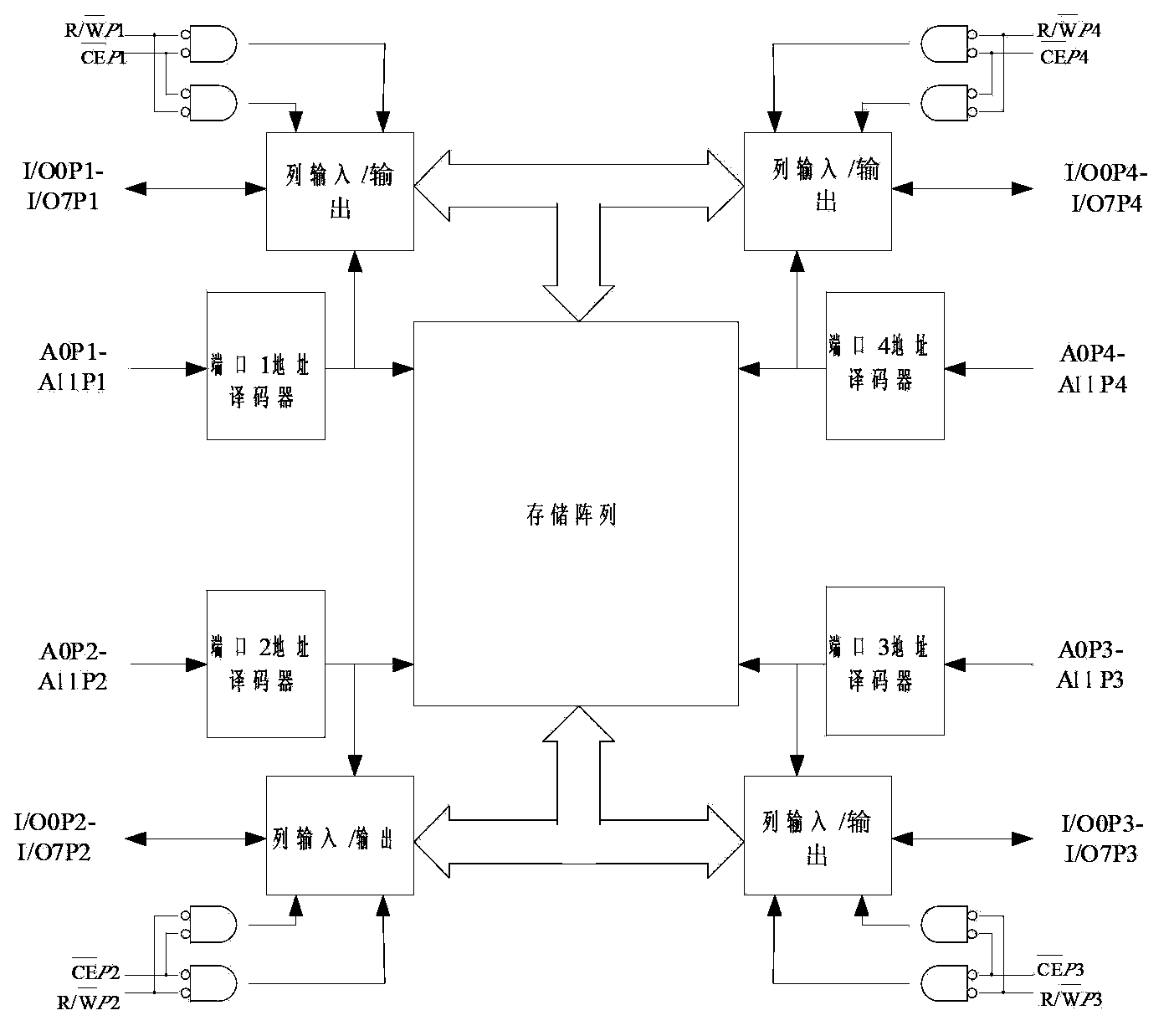
A network-on-chip-based optimization method for DRAM communication comprises the following steps: step 1 , adopting a multi-port SRAM (Static Random Access Memory) to design a multi-port large cache for each input port, adopting the multi-port SRAM as the data cache of PE to construct a plurality of VCs (Virtual Channel) with configurable numbers and depths; step 2, adopting SPQ (Strict Priority Request) method to set transmission priority, namely setting communication between a node and the DRAM as the highest priority, setting inter-nodes communication as the secondary highest priority, providing service for the highest priority first until finished, then providing service for the secondary highest priority. The network-on-chip-based optimization method increases the utility ratio of a memorizer, reduces delay of the whole system, can effectively improve communication quality with an off-chip DRAM, and does not influence the on-chip inter-nodes communication.

Description

technical field [0001] The invention relates to computer multi-core processor architecture, relates to an optimization design and implementation method based on an on-chip network communication architecture, and in particular to an on-chip network-based DRAM communication optimization method. Background technique [0002] With the development of integrated circuit semiconductor technology, more and more processing cores will be integrated on a single chip. The emergence of multi-core chips has gradually shifted the focus of traditional processor research from the pursuit of single-core computing power to the research on on-chip communication capabilities. Then fully organize and explore the parallel processing capability of multi-core chips. The design method of Network-on-Chip (NoC for short) provides an effective solution for the communication interconnection of multi-core chips. [0003] There are two main types of communication in multi-core systems based on network-on-...

Claims


Application Information

Patent Timeline
Patent Type & Authority Applications(China)
IPC IPC(8): G06F13/18G06F15/167
Inventor 任鹏举郑南宁刘卜闵泰任晓伟杨挺孟庆欣葛晨阳
Owner XI AN JIAOTONG UNIV
Learn More