Test method for rapidly exposing welding defects of printed circuit board, and test system thereof

A technology for printed circuit boards and soldering defects, applied in electronic circuit testing, measuring devices, thermal analysis of materials, etc., can solve problems such as printed circuit boards not working properly, substrate deformation of electronic components, and easy desoldering, etc., to improve Effects of market competitiveness, improvement of product quality, and improvement of reliability

Inactive Publication Date: 2013-11-13
OCEANKING DONGGUAN LIGHTING TECH +2
View PDF8 Cites 17 Cited by
  • Summary
  • Abstract
  • Description
  • Claims
  • Application Information

AI Technical Summary

Problems solved by technology

Due to the influence of factors such as working environment and usage habits, the printed circuit board may have substrate deformation after long-term use, and electronic components are prone to desoldering due to welding defects, and abnormalities such as cracking at the soldering point will eventually cause the printed circuit board to fail. normal work

Method used


Image

  • Test method for rapidly exposing welding defects of printed circuit board, and test system thereof

Examples


Embodiment Construction

[0017] In order to further illustrate the principle and structure of the present invention, preferred embodiments of the present invention will now be described in detail with reference to the accompanying drawings.

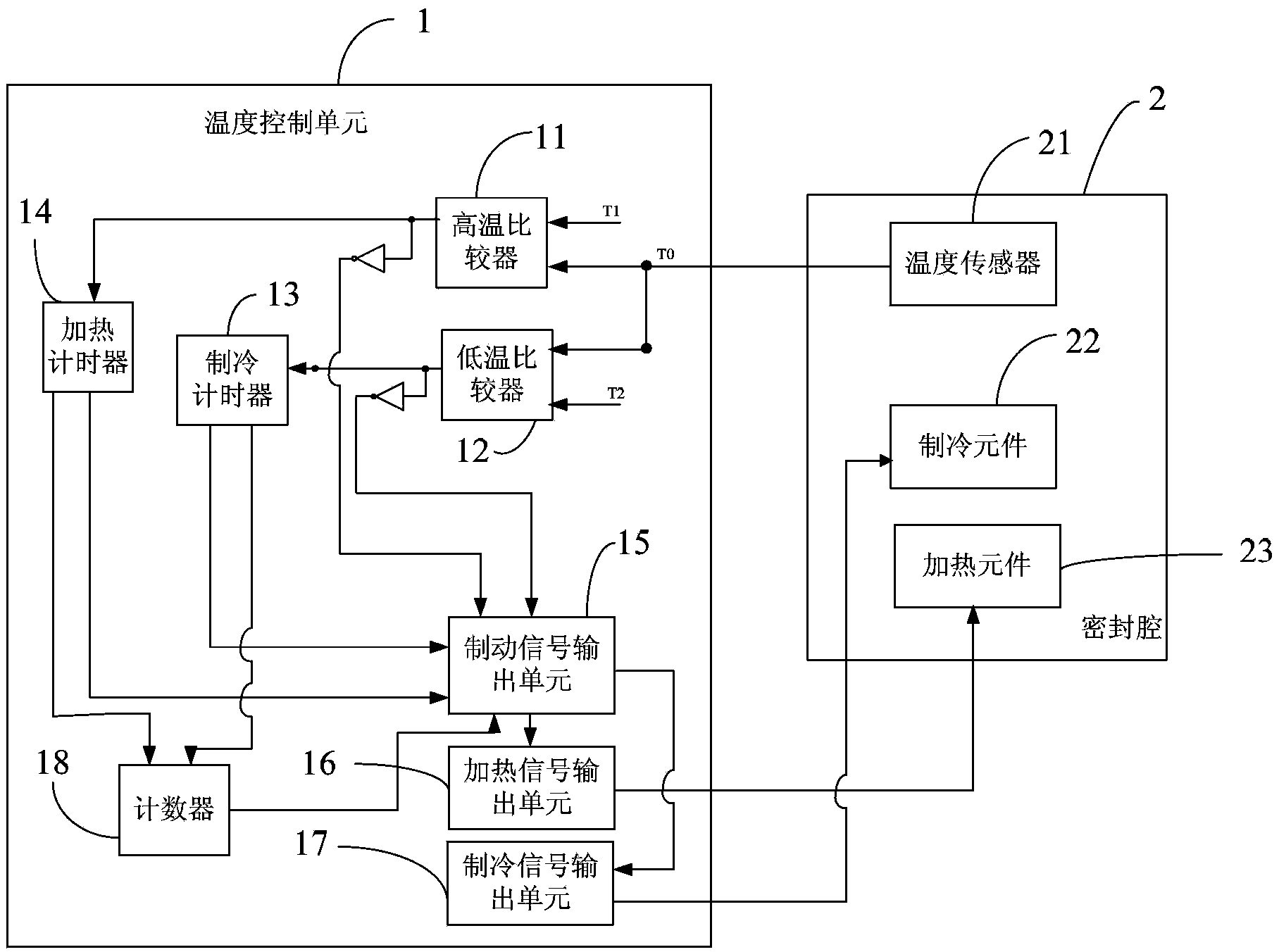
[0018] The test method for quickly exposing soldering defects of printed circuit boards of the present invention mainly includes the following steps: Step 1: Place the printed circuit board sample in a temperature-controlled environment for temperature stress testing, and make the temperature in the environment pass through the low temperature Alternate cycle with high temperature for several times, and make the low temperature and high temperature in each temperature cycle last for a period of time; Step 2: The printed circuit board sample after the temperature stress test is left at room temperature for a period of time, and then the electrical and mechanical properties are tested. Appearance quality inspection, screening out samples with welding defects.

[00...


PUM


Abstract

The invention relates to a test method for rapidly exposing the welding defects of a printed circuit board, and a test system thereof. The test method comprises the following steps: 1, carrying out temperature stress test of printed circuit board samples in the temperature controlled environment, allowing the temperature in the environment to undergo low temperature and high temperature alternative cycle several times, and allowing the low temperature and the high temperature in each of the temperature cycle to last for a period of time respectively; and 2, allowing the printed circuit board samples subjected to the temperature stress test to stand at normal temperature for a period of time, carrying out electric property and appearance quality detection, and screening out samples having welding defects. The test method can detect the welding defects possibly appearing after the printed circuit board is used for a long term within a short period of time, so reliable printed circuit board products are provided for clients.

Description

technical field [0001] The present invention relates to a method and system for testing printing defects of printed circuit boards, in particular to a method and system for exposing possible welding defects of printed circuit boards after long-term use through short-term testing. Background technique [0002] Printed circuit board, also known as printed circuit board, referred to as printed board, or PCB (printed circuit board) or PWB (printed wiring board) in English, is based on an insulating board, cut to a certain size, and has at least one conductive pattern attached to it. , and are equipped with holes (such as component holes, fastening holes, metallized holes, etc.), which are used to replace the chassis of electronic components installed in the past, and to realize the interconnection between electronic components. Since such boards are made using electronic printing, they are called "printed" circuit boards. [0003] Printed circuit boards have been widely used in...

Claims


Application Information

Patent Timeline
Patent Type & Authority Applications(China)
IPC IPC(8): G01N25/00G01R31/28
Inventor 周明杰王永清
Owner OCEANKING DONGGUAN LIGHTING TECH
Why Eureka
Try Eureka