A method of increasing the surface area of ​​an inductor

A surface area and inductance technology, applied in the field of increasing the surface area of ​​inductance, can solve the problems of large winding distance and low density, and achieve the effect of improving performance, large winding density, and increasing effective surface area

Active Publication Date: 2017-11-24
SHANGHAI HUAHONG GRACE SEMICON MFG CORP
View PDF9 Cites 0 Cited by
  • Summary
  • Abstract
  • Description
  • Claims
  • Application Information

AI Technical Summary

Problems solved by technology

[0005] The existing technology proposes a method called Litz winding, which can effectively improve the Q value of the inductor (especially in the case of high frequency). The existing method of realizing Litz winding is to use photolithography and etching However, limited by the lithography size and the ability of the etching process, the distance between the windings realized by this method will be larger and the density will be lower.

Method used


Image

  • A method of increasing the surface area of ​​an inductor
  • A method of increasing the surface area of ​​an inductor
  • A method of increasing the surface area of ​​an inductor

Examples


Embodiment Construction

[0021] In order to make the content of the present invention clearer and easier to understand, the content of the present invention will be described in detail below in conjunction with specific embodiments and accompanying drawings.

[0022] figure 1 A flow chart of a method for increasing the surface area of ​​an inductor according to an embodiment of the present invention is schematically shown.

[0023] Specifically, as figure 1 As shown, the method for increasing the surface area of ​​an inductor according to an embodiment of the present invention includes:

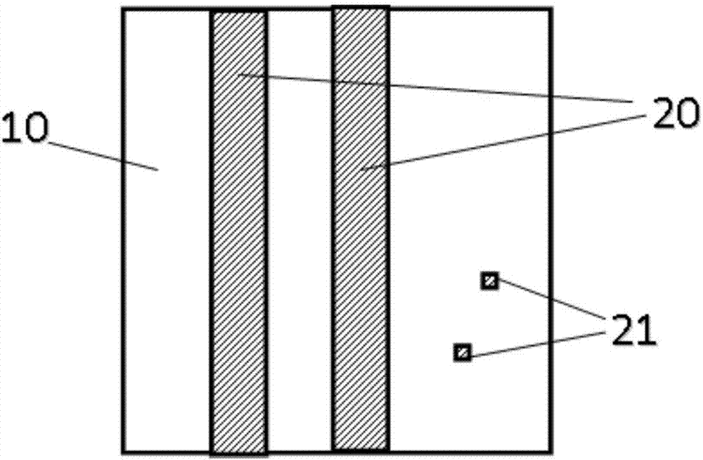
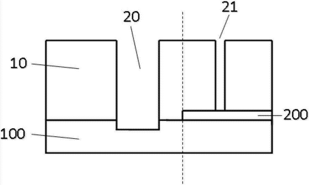
[0024] First step S1: providing a silicon wafer having a first region and a second region, wherein the first region includes a stack of the first oxide layer 100 and the second oxide layer 10, and the second region includes the first oxide layer 100 , the stack of the intermediate metal layer 200 and the second oxide layer 10, such as image 3 As shown in the cross-sectional diagram of , the left side of the dotte...


PUM


Abstract

The invention discloses a method for increasing a surface area of an inductor. The method comprises the steps that a silicon wafer with a first area and a second area is provided, wherein the first area comprises a lamination layer of a first oxide layer and a second oxide layer, and the second area comprises lamination layers of the first oxide layer, a middle metal layer and the second oxide layer; strip-shaped wire lead grooves are etched in the second oxide layer of the first area when circuit wire lead holes are etched in the second area; tungsten layers are formed at the bottoms and on side walls of the strip-shaped lead wire grooves when tungsten is settled in the circuit wire lead holes; aluminum is settled after the tungsten layers are subjected to chemical-mechanical grinding, so that an aluminum layer is formed on the second oxide layer; the strip-shaped lead wire grooves are filled, so that the second oxide layer isolated by the strip-shaped lead wire grooves is connected due to the fact that the strip-shaped lead wire grooves are filled; and gaps formed by the strip-shaped lead wire grooves in the second oxide layer are not filled completely.

Description

technical field [0001] The present invention relates to the field of semiconductor manufacturing, and more particularly, the present invention relates to a method of increasing the surface area of ​​an inductor. Background technique [0002] The skin effect is also known as the "skin effect". Specifically, when an alternating electric current (AC) passes through a conductor, the current distribution on the cross-section of the conductor is uneven due to induction, and the closer to the surface of the conductor, the greater the current density; this phenomenon is called "skin effect". The skin effect increases the effective resistance of a conductor. When a current with a high frequency passes through the wire, it can be considered that the current flows only in a very thin layer on the surface of the wire, which is equivalent to the reduction of the cross-section of the wire and the increase of resistance. [0003] Skin depth means that the current density at this depth is...

Claims


Application Information

Patent Timeline
Patent Type & Authority Patents(China)
IPC IPC(8): H01L21/02H01L21/768
Inventor 黎坡
Owner SHANGHAI HUAHONG GRACE SEMICON MFG CORP
Why Eureka
Try Eureka