

Method for manufacturing three-dimensional through hole interconnection structure based on molten glass skeleton
A technology of molten glass and three-dimensional through-holes, which is applied in semiconductor/solid-state device manufacturing, electrical components, circuits, etc., can solve the problems of weak insulation performance of the growth layer, poor reliability, and difficult electroplating process processing, etc. Simplified process steps and good electrical connection reliability
- Summary
- Abstract
- Description
- Claims
- Application Information
AI Technical Summary
Problems solved by technology
Method used
Image

Examples
Embodiment Construction
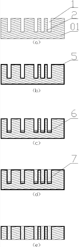
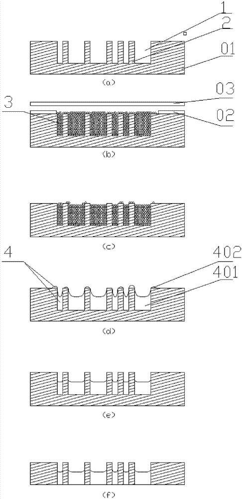
[0024] see figure 2 , the manufacturing process of the embodiment of the three-dimensional through-hole interconnection structure based on the molten glass skeleton according to the present invention includes the following steps:
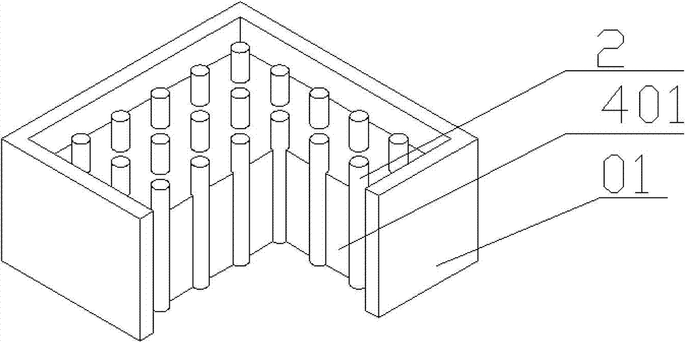
[0025] 1) On the silicon wafer 01, the combined process of photolithography and DRIE is used to process the groove 1 and the silicon pillar 2, such as figure 2 as shown in (a);
[0026] 2) Use the screen plate 02 with a hollow pattern and a thickness of 200 μm to align it with the silicon wafer 01 to ensure that the hollow pattern is aligned with the silicon pillar area of the silicon wafer 01, while the rest of the silicon wafer 01 is protected by the screen plate . Select nano-glass powder 3 (melting point 530°C, thermal expansion coefficient 4.0) and place it in the screen plate 02, use flat plate 03 to reciprocate in the vertical direction, repeatedly squeeze nano-glass powder 3, so that the groove is completely filled with nano-glass powd...
PUM
 Abstract
Description
Claims
Application Information