

A fine metal mask plate for ultra-high resolution evaporation and its manufacturing method
A fine metal mask, ultra-high resolution technology, applied in vacuum evaporation coating, metal material coating process, sputtering coating and other directions, can solve problems such as easy cracking, limit mask resolution, etc. The effect of cracking, improving the resolution of evaporation, and significant industrial application value
- Summary
- Abstract
- Description
- Claims
- Application Information
AI Technical Summary
Problems solved by technology
Method used
Image

Examples
Embodiment 1
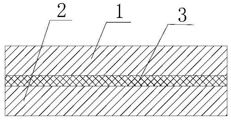
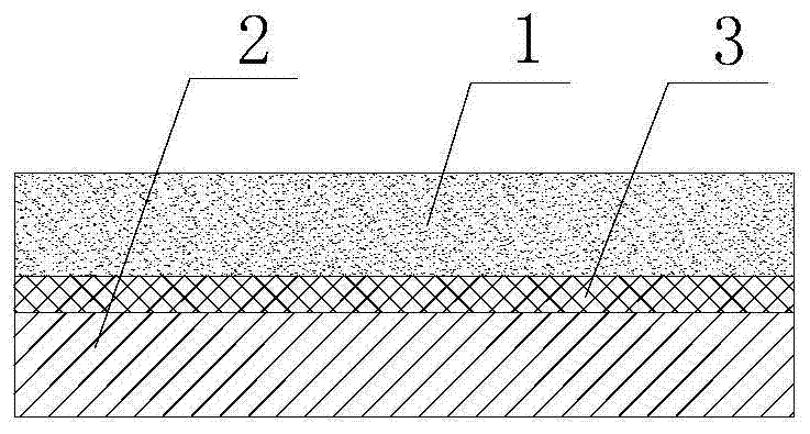
[0030] Such as figure 1 As shown, a kind of fine metal mask plate for ultra-high resolution evaporation provided in this embodiment includes an upper magnetic film layer 1, a lower magnetic film layer 2 and a graphene and / or graphene derivative intermediate layer 3, the upper The magnetic film layer 1, the graphene and / or graphene derivative intermediate layer 3 and the lower magnetic film layer 2 are sequentially stacked to form a sandwich structure.
[0031] Described graphene and / or graphene derivative intermediate layer 3 can adopt roll-to-roll (English is roll toroll, be called for short R2R) method to be laminated on the surface of lower magnetic film layer 2, and upper magnetic film layer 1 can also pass through The lamination method is attached to the surface of the graphene and / or graphene derivative intermediate layer 3, and then the ends of the upper magnetic film layer 1 and the lower magnetic film layer 2 are bonded or welded as one, and then laser-printed hole o...
Embodiment 2
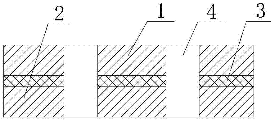
[0035] Such as image 3 As shown, the difference between this embodiment and Embodiment 1 is only that the upper magnetic film layer 1 and the lower magnetic film layer 2 are made of different materials; the upper magnetic film layer 1 is a polyimide film added with soft magnetic metal powder , the lower magnetic film layer 2 is an Invar alloy film, and the soft magnetic metal powder is selected from at least one of Fe, Co, and Ni metal powders. When making through holes, the upper and lower magnetic film layers and the middle layer of graphene and / or graphene derivatives are drilled by laser.
Embodiment 3
[0037] Such as Figure 4 As shown, the difference between this embodiment and Embodiment 1 is only that the upper magnetic film layer 1 and the lower magnetic film layer 2 are made of different materials; the upper magnetic film layer 1 is an Invar alloy film, and the lower magnetic film layer 2 is an additive A polyimide film with soft magnetic metal powder, wherein the soft magnetic metal powder is selected from at least one of Fe, Co and Ni metal powders. When making through holes, the upper magnetic film layer 1 is drilled by wet etching, and the lower magnetic film layer and the middle layer of graphene and / or graphene derivatives are drilled by laser.
PUM
| Property | Measurement | Unit |
|---|---|---|
| thickness | aaaaa | aaaaa |
| thickness | aaaaa | aaaaa |
Abstract
Description
Claims
Application Information