Array substrate, preparing method thereof and display device

An array substrate and a substrate technology are applied in the fields of array substrates and their preparation methods and display devices, which can solve the problems of affecting screen display, occupying pixel area, limited positioning effect of transparent films, etc., so as to reduce storage capacitance and ensure picture quality. Effect

Inactive Publication Date: 2013-11-27
BOE TECH GRP CO LTD
View PDF5 Cites 7 Cited by
  • Summary
  • Abstract
  • Description
  • Claims
  • Application Information

AI Technical Summary

Problems solved by technology

like figure 1 As shown, the storage capacitance (Cst) of the common electrode 111 and the pixel electrode 112 of the TFT array substrate 110 in the ADS mode is very large, almost occupying the entire pixel area, especially for large-sized products, due to the larger pixel area, the storage capacitance It will become larger. Usually, in order to adapt to such a large storage capacitor, it is necessary to design a larger thin film transistor for filling. The larger thin film transistor will occupy the pixel area, and the second is the coupling capacitance Cgd, Cgs of the thin film transistor itself. will become larger, which will affect the display of the screen, and thus be subject to many restrictions in design. Generally, one of the most direct methods to solve such problems is to form the ADS type pixel electrode 112 and the common electrode 111 as figure 2 The state shown, but the current process cannot be directly realized, because the pixel electrode 112 and the common electrode 111 are both transparent electrodes, and the alignment effect of the transparent film is limited during the process of exposing and developing through process equipment. , the device simply cannot be truly as figure 2 In the structure shown, if the relative displacement between the pixel electrode and the common electrode is not uniform in an effective display area due to process alignment deviation, for example, the pixel electrode 112 in a part of the area is deflected to the left relative to the common electrode 111, while the pixel electrode 112 in another part of the area is biased to the left. Relative to the common electrode 111 to the right, there will be unevenness between Cst regions, which will be reflected in the screen, and the display grayscale between various regions on a display will be uneven, and what the human eye feels is the display between the screen regions. Uneven brightness leads to picture distortion, which is a very fatal display defect, and there is no good solution in the prior art

Method used


Image

  • Array substrate, preparing method thereof and display device
  • Array substrate, preparing method thereof and display device
  • Array substrate, preparing method thereof and display device

Examples


Embodiment Construction

[0048] In order to make the technical problems, technical solutions and advantages to be solved by the present invention clearer, the following will describe in detail with reference to the drawings and specific embodiments.

[0049] An embodiment of the present invention provides a method for preparing an array substrate, including:

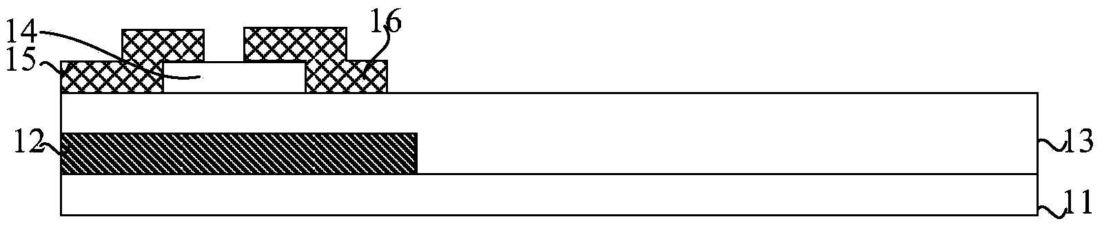
[0050] A common electrode with a slit structure and a pixel electrode with a slit structure zero-overlapping with the common electrode are formed on the substrate.

[0051]In this embodiment, a common electrode with a slit structure and a pixel electrode with a slit structure with zero overlap with the common electrode are formed on the substrate, thereby reducing storage capacitance between the common electrode and the pixel electrode and ensuring picture quality.

[0052] Such as image 3 - Figure 8 As shown, the above-mentioned common electrode with a slit structure formed on the substrate, and the specific implementation process of the pi...


PUM


Abstract

The invention provides an array substrate, a preparing method thereof and a display device. The preparing method of the array substrate comprises the steps that a public electrode and a pixel electrode are formed on the substrate, the public electrode is of a slit structure, and the pixel electrode is of a slit structure and has no overlap with the public electrode. According to the scheme, storage capacitance of the public electrode and storage capacitance of the pixel electrode can be reduced, and image quality is guaranteed.

Description

technical field [0001] The present invention relates to the field of display technology, in particular to an array substrate, a preparation method thereof, and a display device. Background technique [0002] TFT-LCD (Thin Film Transistor-Liquid Crystal Display, Thin Film Field Effect Transistor Liquid Crystal Display) uses the change of the electric field intensity set on the liquid crystal layer to change the degree of rotation of liquid crystal molecules, thereby controlling the intensity of light transmission to display images . Generally speaking, a complete liquid crystal display panel must have a backlight module group, a polarizer, an upper substrate (usually a color filter substrate), a lower substrate (usually an array substrate), and a box filled with the two substrates. Layers of liquid crystal molecules. [0003] On the array substrate, data lines and gate lines intersecting horizontally and vertically are formed, and the data lines and gate lines surround pixe...

Claims


Application Information

Patent Timeline
Patent Type & Authority Applications(China)
IPC IPC(8): H01L21/77G02F1/1343G02F1/1362G02F1/1368
CPCG02F1/134309G02F1/134372H01L27/124H01L27/1248H01L27/1255H01L27/1259H01L27/1288G02F1/136286G02F1/1368G02F1/13685
Inventor 崔承镇金熙哲宋泳锡刘圣烈
Owner BOE TECH GRP CO LTD
Why Eureka
Try Eureka