

Semiconductor device packing structure and semiconductor device packing technological process
A technology of packaging structure and process flow, which is applied in the direction of semiconductor devices, semiconductor/solid-state device components, semiconductor/solid-state device manufacturing, etc., can solve the problems of semiconductor devices occupying a large area and complex processes, etc., to reduce the overall area and simplify Packaging process, the effect of improving flexibility
- Summary
- Abstract
- Description
- Claims
- Application Information
AI Technical Summary
Problems solved by technology
Method used
Image

Examples
Embodiment Construction
[0056] The following will clearly and completely describe the technical solutions in the embodiments of the present invention with reference to the accompanying drawings in the embodiments of the present invention. Obviously, the described embodiments are only some, not all, embodiments of the present invention. All other embodiments obtained by persons of ordinary skill in the art based on the embodiments of the present invention belong to the protection scope of the present invention.
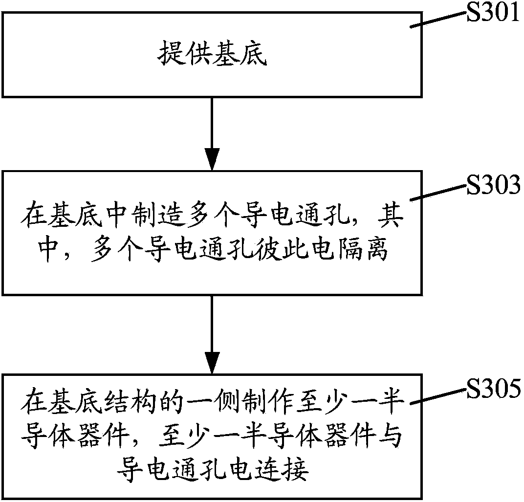
[0057] According to an embodiment of the present invention, a packaging structure of a semiconductor device is provided.
[0058] A package structure of a semiconductor device according to an embodiment of the present invention includes:
[0059] a substrate, the substrate has a plurality of conductive vias electrically isolated from each other, at least part of each conductive via is located in the substrate, and the portion of each conductive via in the substrate is separated from the The ...
PUM
 Abstract
Description
Claims
Application Information