Intelligent test system and test method for improving probe card test abnormality

A test system and test method technology, applied in the direction of electronic circuit testing, etc., can solve the problems of reduced contact ability, shortened probe length, large diameter, etc., so as to improve abnormal chip parameter test results, ensure contact ability, and improve pass rate Effect

Inactive Publication Date: 2013-12-11
SHANGHAI HUALI MICROELECTRONICS CORP
View PDF8 Cites 15 Cited by
  • Summary
  • Abstract
  • Description
  • Claims
  • Application Information

AI Technical Summary

Problems solved by technology

[0006] In view of the above existing problems, the present invention discloses an intelligent test system and a test method for improving probe card test abnormalities, so as to overcome the consumption of the probe card in the prior art, the length of the probe is shortened, and the diameter is enlarged. Reduced contact ability, and the problem of wire aging

Method used


Image

  • Intelligent test system and test method for improving probe card test abnormality
  • Intelligent test system and test method for improving probe card test abnormality
  • Intelligent test system and test method for improving probe card test abnormality

Examples


Embodiment Construction

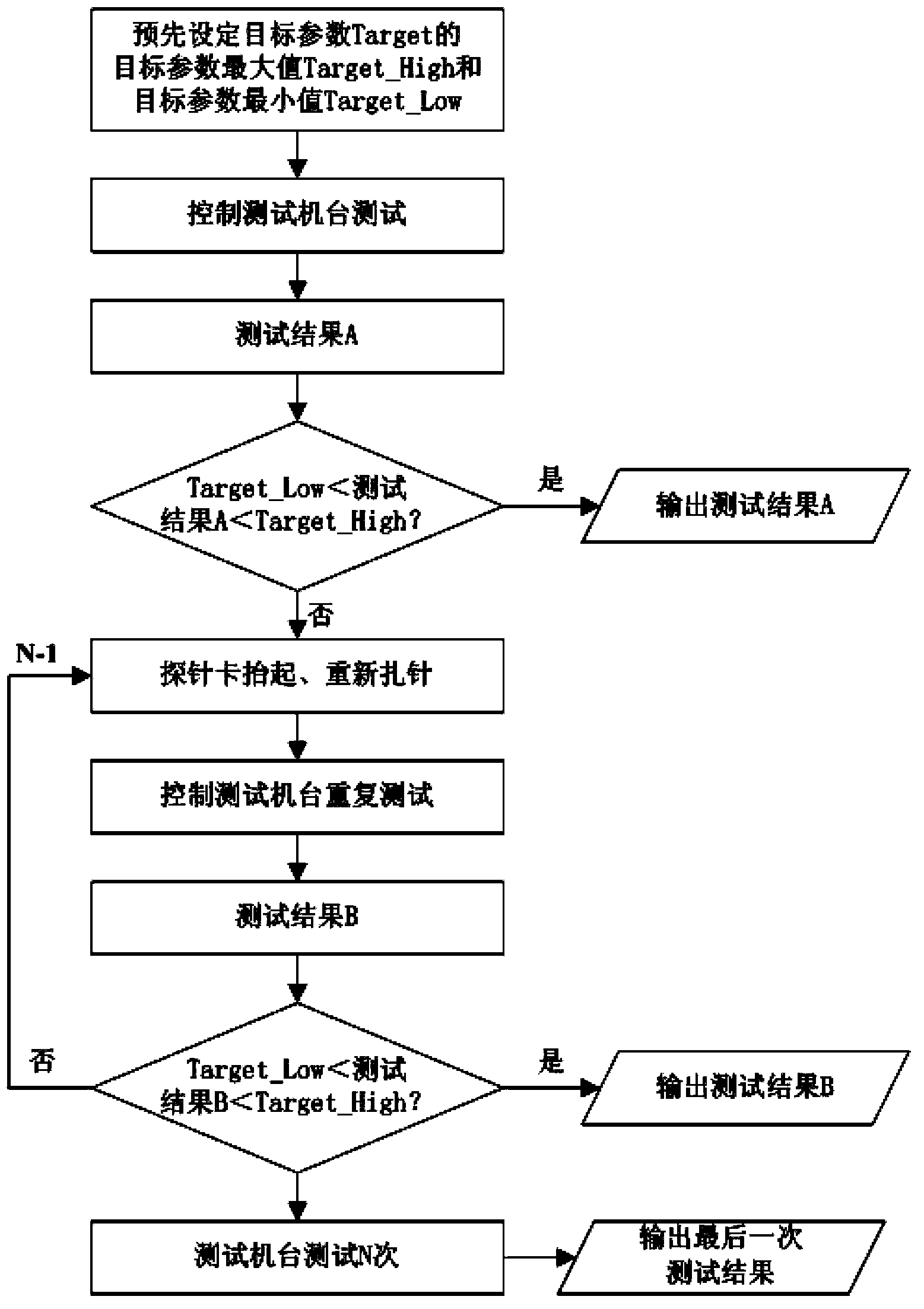
[0037] The present invention will be further described below in conjunction with the accompanying drawings and specific embodiments, but not as a limitation of the present invention.

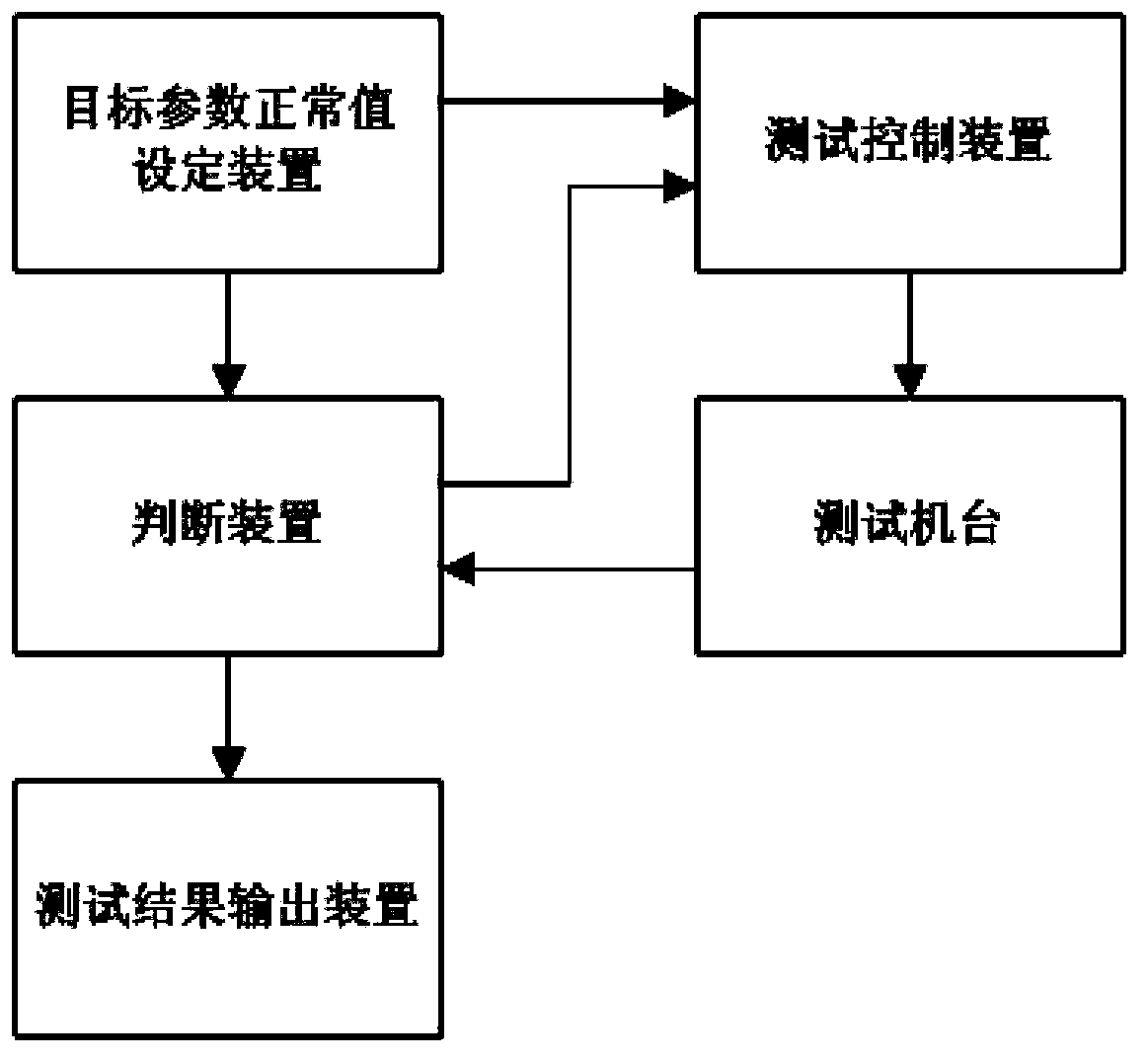
[0038] The first embodiment of the present invention relates to an intelligent test system for improving probe card test abnormalities, which is applied to chip parameter testing, such as figure 1 As shown, it includes a test machine with a probe card, wherein the probe card of the test machine is connected to the bonding pad of the chip, and also includes: a target parameter normal value setting device, a test control device connection, a judging device, and a test Result output device.

[0039] The target parameter normal value setting device is respectively connected with the judging device and the test control device, and is pre-set by the target parameter normal value setting device. After the target parameter normal value is set, the target parameter normal value setting device sends the t...


PUM


Abstract

The invention discloses an intelligent test system for improving probe card test abnormality. The intelligent test system is applied to a test of chip parameters and comprises a testing machine stand provided with a probe card. The intelligent test system further comprises a target parameter normal value setting device, a judging device, a test result output device and a test control device. The invention further discloses a test method for improving the probe card test abnormality. The method further includes the following steps of target parameter normal value setting, testing and controlling, judging, test result outputting and repeated testing and controlling. According to the intelligent test system and the test method for improving the probe card test abnormality, through repeated probing, testing and parameter range judging, consumption of the probe card is effectively reduced, the contact capacity of the probe card is guaranteed, wire rod aging of the probe card is controlled, therefore, the problem that due to the probe card test abnormality, chip parameter test results are abnormal is improved, and the qualified rate of chip testing is improved.

Description

technical field [0001] The invention relates to the field of microelectronics technology, in particular to the field of wafer chip parameter testing, in particular to an intelligent testing system and a testing method for improving probe card testing abnormalities. Background technique [0002] At present, all test parameters are completed with a single needle test, and the probe card as a test bridge plays a key role in both test accuracy and test stability, but the cost price of a probe card is different. Fei, excessive use will cause consumption of the probe card, the length of the probe will be shortened, the diameter will become larger, the contact ability will be reduced, and the wire will be aged. At this time, the test chip parameter pass rate (Pass Rate) will be greatly reduced , especially when testing sensitive parameters, it will cause certain instability. [0003] Chinese patent (publication number: CN101452010) discloses a probe card for chip testing, includin...

Claims


Application Information

Patent Timeline
Patent Type & Authority Applications(China)
IPC IPC(8): G01R31/28
Inventor 沈茜周波
Owner SHANGHAI HUALI MICROELECTRONICS CORP
Why Eureka
Try Eureka