Three-dimensional system-level chip normal installation stacking packaging structure formed by sealing first and then corroding and technique method

A system-level chip, first sealing and then etching technology, applied in the manufacturing of electrical components, electric solid state devices, semiconductor/solid state devices, etc., can solve problems such as difficulty in controlling the quality of interconnecting solder balls between packages

Active Publication Date: 2013-12-11
江阴芯智联电子科技有限公司
View PDF3 Cites 6 Cited by
  • Summary
  • Abstract
  • Description
  • Claims
  • Application Information

AI Technical Summary

Problems solved by technology

[0008] The purpose of the present invention is to overcome the above-mentioned shortcomings, and provide a three-dimensional system-in-package struct

Method used


Image

  • Three-dimensional system-level chip normal installation stacking packaging structure formed by sealing first and then corroding and technique method
  • Three-dimensional system-level chip normal installation stacking packaging structure formed by sealing first and then corroding and technique method
  • Three-dimensional system-level chip normal installation stacking packaging structure formed by sealing first and then corroding and technique method

Examples


Embodiment 1

[0171] Example 1: Single-layer circuit

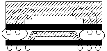
[0172] see Figure 24 , the present invention is a three-dimensional system-on-a-chip stacked packaging structure that is sealed first and etched later. It includes a base island 1 and pins 2. The front side of the pin 2 is provided with a conductive pillar 3. The front side of the base island 1 is connected by conducting or not The conductive adhesive substance 6 is equipped with the chip 4, and the front of the chip 4 is connected with the front of the pin 2 through the metal wire 5, the front area of ​​the base island 1 and the pin 2 and the conductive pillar 3, the chip 4 and the metal wire 5 the peripheral area is encapsulated with molding compound or epoxy resin 7, the molding compound or epoxy resin 7 is flush with the top of the conductive pillar 3, the base island 1 and the back of the pin 2 are provided with a highly conductive metal layer 11, Green paint or photosensitive non-conductive adhesive material 12 is filled between...

Embodiment 2

[0220] Embodiment 2: multi-layer circuit

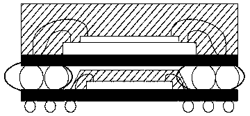
[0221] see Figure 72 , the present invention is a three-dimensional system-on-a-chip stacked packaging structure that is sealed first and etched later. It includes a base island 1 and pins 2. The front side of the pin 2 is provided with a conductive pillar 3. The front side of the base island 1 is connected by conducting or not The conductive bonding substance 6 is equipped with the chip 4, and the front of the chip 4 is connected with the front of the pin 2 through the metal wire 5, and the area of ​​the front of the base island 1 and the pin 2 and the conductive pillar 3, the chip 4 and the metal The area around the line 5 is encapsulated with a molding compound or epoxy resin 7, the molding compound or epoxy resin 7 is flush with the top of the conductive pillar 3, and the base island 1 and the back of the pin 2 are provided with a highly conductive metal layer 11. Green paint or photosensitive non-conductive adhesive material 12...

Embodiment 3

[0318] Example 3: Single-layer circuit + backside stacked L-shaped package with pins

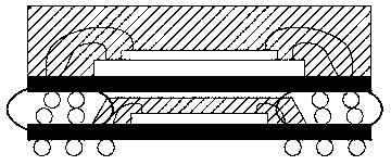
[0319] see Figure 73 The difference between embodiment 3 and embodiment 1 is that the package body 10 is stacked on the anti-oxidation layer on the back of the pin.


PUM

PropertyMeasurementUnit
Thicknessaaaaaaaaaa

Abstract

The invention relates to a three-dimensional system-level chip normal installation stacking packaging structure formed by sealing first and then corroding and a technique method. The packaging structure comprises a paddle (1) and pins (2). Electricity conducting columns (3)are arranged on front faces of the pins (2). A chip (4) is arranged on the front face of the paddle (1) through electricity-conducting or non-electricity-conducting adhesive substances. The front face of the chip (4) is connected with front faces of the pins (2) through metal wires (5). Plastic packaging materials or epoxy resin (7) wraps the area of the front face of the paddle (1), areas of the front faces of the paddles (2) and the peripheral area of the electricity conducting columns(3), the peripheral area of the chip (4), and the peripheral area of the metal wires (5). Anti oxidation layers (8) are arranged on the surface, exposing out of the plastic packaging materials or the epoxy resin (7), of the paddle (1), the surfaces, exposing out of the plastic packaging materials or the epoxy resin (7), of the pins (2), and the surfaces, exposing out of the plastic packaging materials or epoxy resin (7), of the electricity conducting columns (3). Packaging bodies (10) are stacked at tops of the electricity conducting columns (3) through electricity conducting substances (9). The packaging structure has the advantages of solving the problem that the quality of interconnected solder balls between packaging bodies is hard to control due to the fact that a lower layer welding disk is lower than a lower layer plastic packaging face in traditional substate packaging stacking.

Description

technical field [0001] The invention relates to a three-dimensional system-level chip front-mount stack packaging structure and a process method after sealing first and etching later, and belongs to the technical field of semiconductor packaging. Background technique [0002] The traditional common PoP package stacking structure is that the bottom logic device substrate package is stacked with the top layer storage device substrate package, and the bottom layer device and the top layer device are stacked and electrically interconnected by solder ball mounting and reflow soldering ( Such as Figure 80 shown). [0003] The above PoP (Package on Package) packaging structure has the following disadvantages: [0004] 1. The pads connecting the bottom package and the top package are located on the substrate of the bottom package, which is lower than the plastic cover of the bottom package, so the molding height of the bottom package is limited by the size of the metal solder ball...

Claims


Application Information

Patent Timeline
IPC IPC(8): H01L21/48H01L21/56H01L23/495H01L23/31
CPCH01L2224/48091H01L2224/73265H01L2224/92247H01L2924/181H01L2924/00014H01L2924/00012
Inventor 梁志忠王亚琴王孙艳林煜斌廖小景
Owner 江阴芯智联电子科技有限公司
Why Eureka
Try Eureka