Organic electroluminescence device
An electroluminescent element and electroluminescent technology, applied in electroluminescent light sources, electrical components, organic semiconductor devices, etc., can solve the problems of reduced reliability, uneven film thickness, easy occurrence of short circuits, etc. The effect of the loss of light
- Summary
- Abstract
- Description
- Claims
- Application Information
AI Technical Summary
Problems solved by technology
Method used
Image

Examples
Embodiment 1)
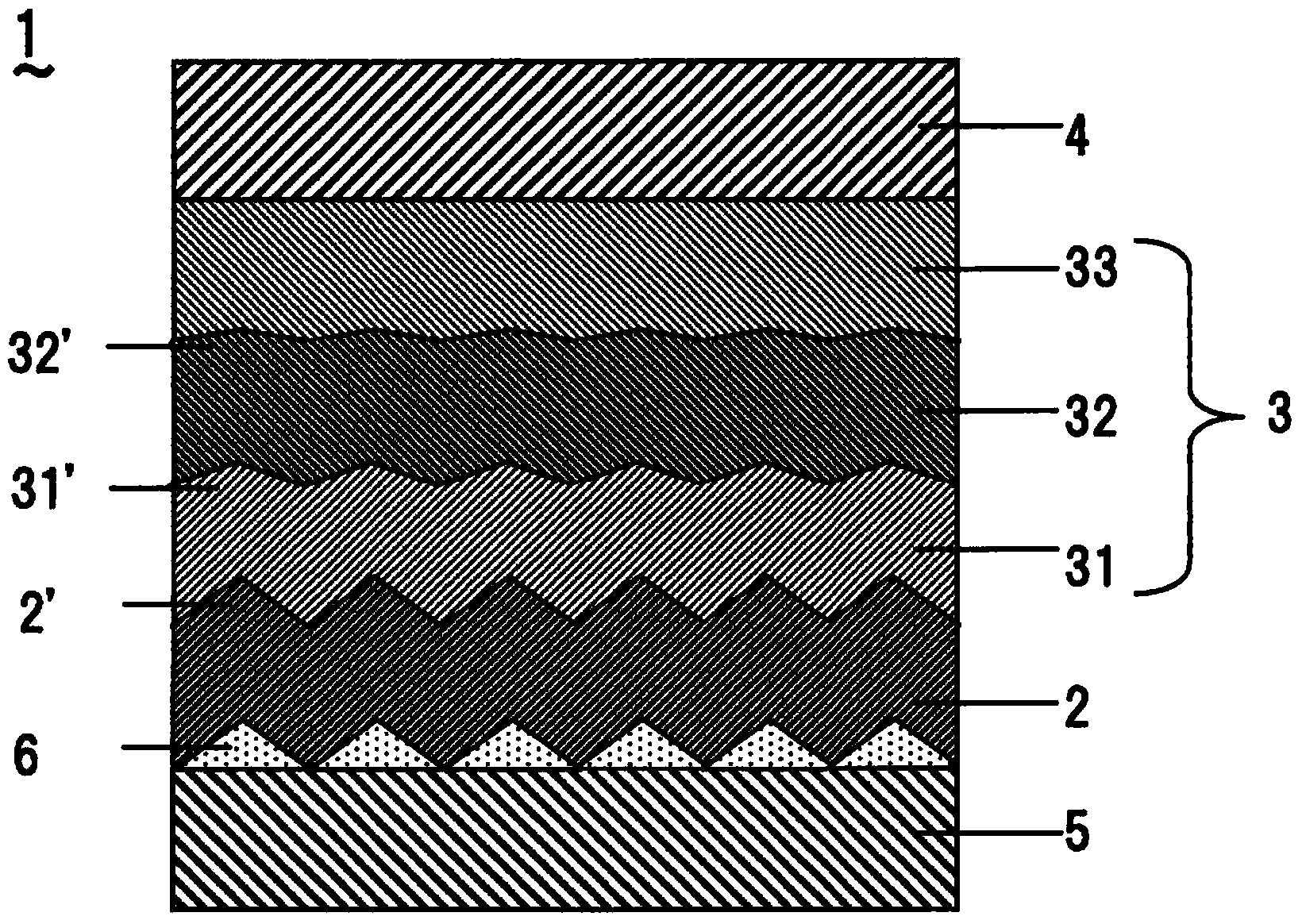
[0056] Example 1 and figure 1 The illustrated organic EL element 1 of the first embodiment corresponds to it. As the substrate 5 , an alkali-free glass plate (No. 1737; manufactured by Corning) having a thickness of 0.7 mm was used, and polymethyl methacrylate (PMMA) as a thermoplastic resin was coated thereon. After that, using a mold formed with triangular grooves with a depth of 50nm and a pitch of 200nm, the temperature is raised to 105°C or higher, which is the glass transition temperature of PMMA, and the mold is crimped. After cooling, the mold is separated from the substrate 5, whereby the mold pattern is separated. By transferring to the resin, fine irregularities 6 in the shape of triangular grooves with a height of 50 nm and a pitch of 200 nm are formed on the substrate 5 .
[0057] Aluminum was deposited as a metal layer 2 with a thickness of 80 nm on the substrate 5 on which the unevenness 6 was formed by a vacuum evaporation method, and was used as a cathode. ...
Embodiment 2)
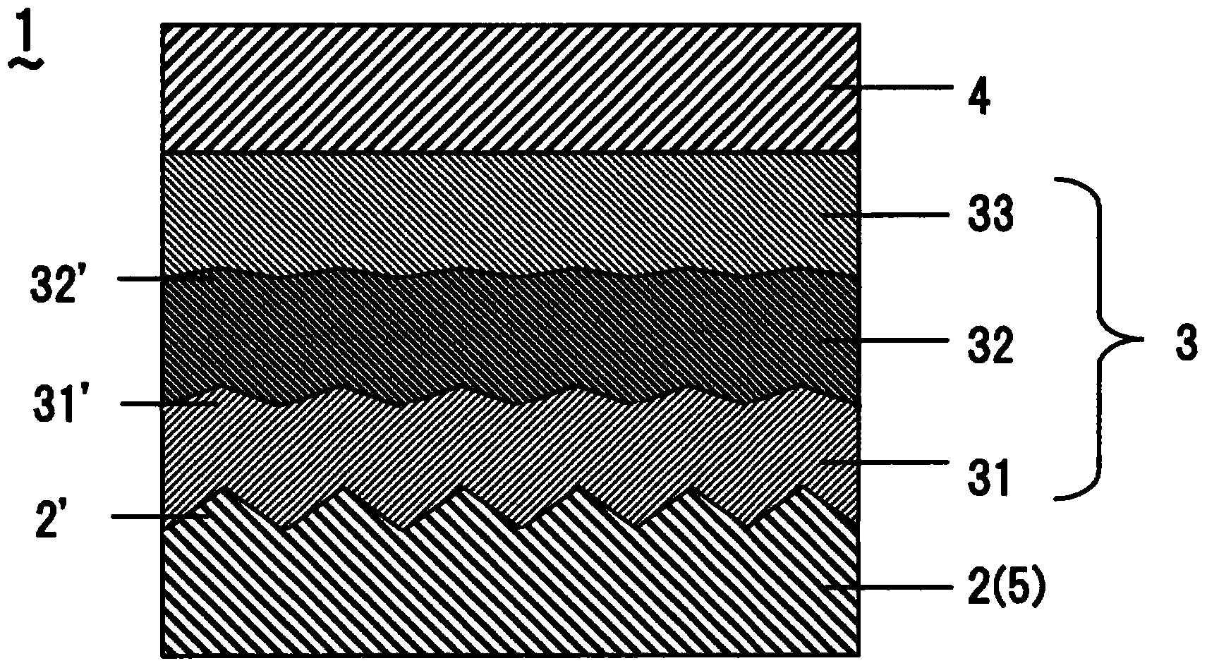
[0060] Example 2 corresponds to figure 2 The organic EL element 1 of the 2nd Embodiment shown. Aluminum foil (approximately 30 μm thick) was used as the metal layer 2 (substrate), and the same mold as in Example 1 was crimped on the smooth surface side to form fine irregularities 2' in the same triangular groove shape as in Example 1 on the aluminum foil. The light emitting layer 31 was formed on this aluminum foil by the same method as in Example 1. Other than that, the organic EL element 1 was produced in the same manner as in Example 1.
Embodiment 3)
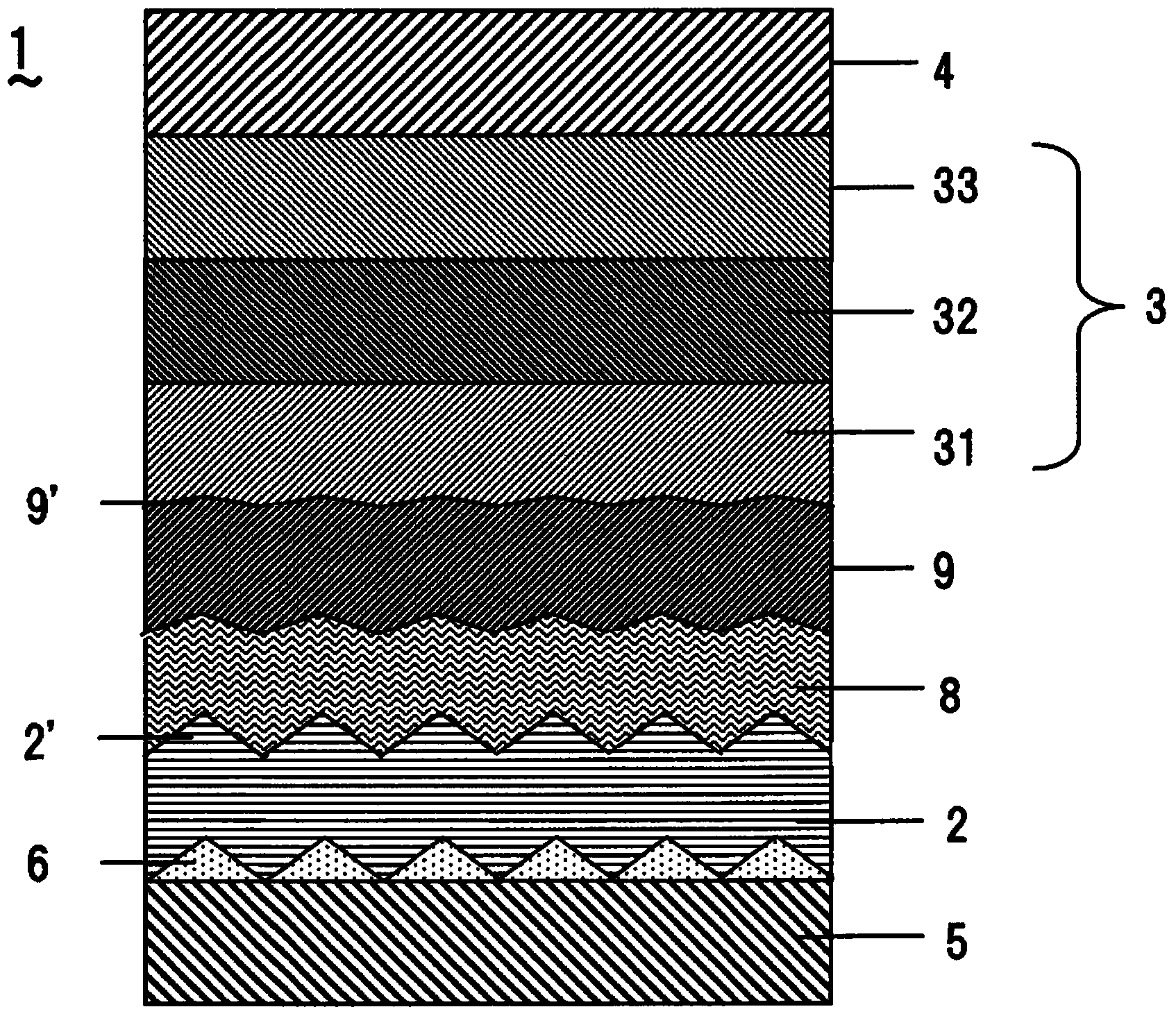
[0062] Example 3 corresponds to image 3 The organic EL element 1 of the 3rd Embodiment shown. As the substrate 5 , an alkali-free glass plate (No. 1737; manufactured by Corning) having a thickness of 0.7 mm was used, and polymethyl methacrylate (PMMA) as a thermoplastic resin was coated thereon. After that, using a mold formed with triangular grooves with a depth of 50nm and a pitch of 200nm, the temperature is raised to 105°C or higher, which is the glass transition temperature of PMMA, and the mold is crimped. After cooling, the mold is separated from the substrate 5, whereby the mold pattern is separated. By transferring to the resin, fine irregularities 6 in the shape of triangular grooves with a height of 50 nm and a pitch of 200 nm are formed on the substrate 5 . Next, aluminum is formed into a film with a thickness of 80 nm on the substrate 5 on which the unevenness 6 is formed by vacuum evaporation to form a metal layer 2 as a reflective layer, and PMMA 100 nm is coa...
PUM
| Property | Measurement | Unit |
|---|---|---|
| Height | aaaaa | aaaaa |
| Thickness | aaaaa | aaaaa |
| Thickness | aaaaa | aaaaa |
Abstract
Description
Claims
Application Information
 - R&D
- Intellectual Property
- Life Sciences
- Materials
- Tech Scout
- Unparalleled Data Quality
- Higher Quality Content
- 60% Fewer Hallucinations
Browse by: Latest US Patents, China's latest patents, Technical Efficacy Thesaurus, Application Domain, Technology Topic, Popular Technical Reports.
© 2025 PatSnap. All rights reserved.Legal|Privacy policy|Modern Slavery Act Transparency Statement|Sitemap|About US| Contact US: help@patsnap.com