Packaging-after etching three-dimensional system-on-chip upright stacking packaging structure and technology method

A system-level chip, etch first and then seal technology, applied in the direction of semiconductor/solid-state device parts, semiconductor devices, electrical components, etc., can solve the problem of difficult to control the quality of interconnecting solder balls between packages

Active Publication Date: 2013-12-18
江苏尊阳电子科技有限公司
View PDF6 Cites 8 Cited by
  • Summary
  • Abstract
  • Description
  • Claims
  • Application Information

AI Technical Summary

Problems solved by technology

[0009] The purpose of the present invention is to overcome the above-mentioned shortcomings, and provide a three-dimensional system-in-package structure and process method for sealing first and then etching chips, which can solve t...

Method used


Image

  • Packaging-after etching three-dimensional system-on-chip upright stacking packaging structure and technology method
  • Packaging-after etching three-dimensional system-on-chip upright stacking packaging structure and technology method
  • Packaging-after etching three-dimensional system-on-chip upright stacking packaging structure and technology method

Examples


Embodiment 1

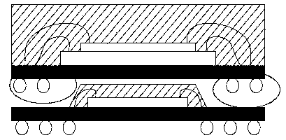
[0201] Embodiment 1. Single-layer circuit single-chip formal mounting single-turn pins

[0202] See Figure 27 , Is a schematic structural view of Embodiment 1 of the three-dimensional system-on-chip front-mount stack package structure of the present invention, which is etched and then sealed. It includes a base island 1 and a pin 2. The front surface of the base island 1 is provided with a conductive or non-conductive adhesive material 3 There is a chip 4, the front surface of the chip 4 and the front surface of the pin 2 are connected by a metal wire 5, and a conductive pillar 6 is provided on the front surface of the pin 2. The peripheral area of ​​the base island 1 and the base island 1 The area between pin 2 and pin 2, the area between pin 2 and pin 2, the area above base island 1 and pin 2, the area below base island 1 and pin 2, and the chip 4, metal line 5 and The conductive pillars 6 are all encapsulated with a plastic molding compound 7. The plastic molding compound 7 i...

Embodiment 2

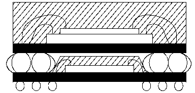
[0256] Embodiment 2. Stacked J-shaped foot package

[0257] See Figure 28 , Is a schematic structural diagram of Embodiment 2 of the three-dimensional system-on-chip front-mount stacked package structure of the present invention, which is etched and then sealed. The difference between Embodiment 2 and Embodiment 1 is that the outer corner of the package body 9 is a J-shaped foot.

Embodiment 3

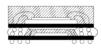
[0258] Embodiment 3. Stacked L-shaped foot package

[0259] See Figure 29 , Is a schematic structural diagram of Embodiment 3 of the three-dimensional system-on-chip front-mount stack package structure of the present invention, which is etched and then sealed. The difference between Embodiment 3 and Embodiment 1 is that the outer corner of the package body 9 is an L-shaped foot.


PUM

PropertyMeasurementUnit
Thicknessaaaaaaaaaa

Abstract

The invention relates to a packaging-after etching three-dimensional system-on-chip upright stacking packaging structure and a technology method. The packaging-after etching three-dimensional system-on-chip upright stacking packaging structure comprises a base island and pins, a chip is arranged in the front of the base island through conducting materials and non-conducting materials; the front of the chip is connected with the fronts of the pins through metal wires; conducting posts are arranged in the fronts of the pins; the region on the periphery of the base island, the region between the base island and the pins, the region between the pins, the region above the base island and the pins, the region below the base island and the pins, the chip, the metal wires and the conducting posts are all wrapped with molding compounds; packaging bodies are arranged on the tops of the conducting posts or the backs of the pins through conducting materials. The e packaging-after etching three-dimensional system-on-chip upright stacking packaging structure and the technology method have the advantages of solving the problem that because a bottom-layer substrate welding disc is lower than a bottom-layer plastic packing surface in a traditional substrate packaging stacking mode, the quality of interconnected welding balls between the packaging bodies is hard to control.

Description

Technical field [0001] The invention relates to a three-dimensional system-level chip front-mounting stacked packaging structure and a process method after etching and sealing. It belongs to the field of semiconductor packaging technology. Background technique [0002] The traditional and common PoP package stack structure is to stack the top storage device substrate package on the bottom logic device substrate package. The bottom device and the top device are mounted on solder balls and reflow soldering to achieve the stacking and electrical interconnection of the two packages. Such as Figure 81 . [0003] The aforementioned PoP (Package on Package) packaging structure has the following shortcomings: [0004] 1. The interconnecting pad between the bottom package and the top package is located on the substrate of the bottom package, lower than the plastic cover of the bottom package, so the molding height of the bottom package is limited by the size of the metal tin ball on the bot...

Claims


Application Information

Patent Timeline
IPC IPC(8): H01L21/48H01L21/56H01L23/495H01L23/31
CPCH01L23/49513H01L23/49517H01L23/49811H01L23/49816H01L23/49822H01L21/4825H01L21/4853H01L25/105H01L2224/48091H01L2224/73265H01L2224/83192H01L2224/92247H01L23/3107H01L21/561H01L21/568H01L2924/181H01L2225/1029H01L2225/1058H01L2924/00014H01L2924/00012H01L21/4828H01L21/4842H01L21/4889H01L21/565H01L23/3178H01L23/4952H01L23/49575H01L25/0657H01L25/50H01L2225/0651H01L2225/06517H01L2225/06541H01L2225/06582
Inventor 梁志忠王亚琴章春燕林煜斌张友海
Owner 江苏尊阳电子科技有限公司
Why Eureka
Try Eureka