Novel semiconductor packaging method

A packaging method and semiconductor technology, which is applied in the direction of semiconductor devices, semiconductor/solid-state device manufacturing, electric solid-state devices, etc., to achieve strong support, good thermal shock resistance and water vapor shock performance, and low impedance

Inactive Publication Date: 2013-12-25
HUIZHOU SPEED WIRELESS TECH CO LTD
View PDF6 Cites 3 Cited by
  • Summary
  • Abstract
  • Description
  • Claims
  • Application Information

AI Technical Summary

Problems solved by technology

Such interconnects suffer from homogeneity in solder bumps and in thermal expansion mismatch, which limits the available substrates to silicon or materials with similar thermal expansion characteristics to silicon

Method used


Image

  • Novel semiconductor packaging method
  • Novel semiconductor packaging method
  • Novel semiconductor packaging method

Examples


Embodiment Construction

[0057] In order to make it easier for those skilled in the art to understand the technical content of the present invention, the present invention will be further described in detail below in conjunction with the embodiments and accompanying drawings.

[0058] The semiconductor packaging method disclosed in the present invention comprises the steps of:

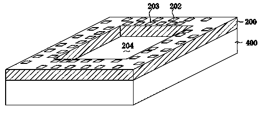
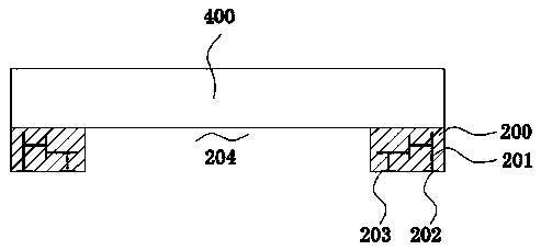
[0059] (1) Provide a wafer with a functional area 101 and a substrate, each chip 100 of the wafer is provided with a metal contact 102;

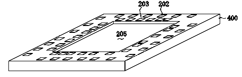
[0060] (2) The substrate may be a multi-layer substrate or a single-layer substrate, such as a glass substrate or a printed circuit board. Such as figure 1 and 2As shown, it is a two-layer substrate composed of a glass substrate 400 and a printed circuit board 200. Metal pads are made on the same side of the substrate, and the metal pads include an inner ring metal pad 203 and an outer ring metal pad 202. The ring metal pad 203 corresponds to the position of the metal contact 102 on the c...


PUM


Abstract

The invention discloses a novel semiconductor packaging method. According to the method, a circle of inner ring metal cushions and a circle of outer ring metal cushions are manufactured on the same lateral side of a substrate, the inner ring metal cushions correspond to metal contacts on chips in position, the inner ring metal cushions are communicated with the outer ring metal cushions respectively in a paired mode in the substrate, metal lugs are manufactured on the metal contact of each chip and / or on each inner ring metal cushion respectively, the chips are welded on the substrate in an inversed mode, metal circuits and metal welding pads which are communicated with the outer ring metal cushions are manufactured on the back sides of the chips, input and output metal protruding points are manufactured on the metal welding pads, and then the packaging of the chips is achieved. According to the novel semiconductor packaging method, the metal lugs are directly manufactured on the metal contacts of the chips or on the inner ring metal cushions of the substrate, the chips are welded on the substrate in the inversed mode, a silicon layer below the metal contact of each chip is complete, supporting force is firmer, the rupture phenomenon is avoided, and thermal shock resistance and moisture shock resistance of products are better.

Description

technical field [0001] The invention relates to semiconductor packaging, in particular to a novel semiconductor packaging method. Background technique [0002] A critical step in the fabrication of integrated circuit devices is called "packaging," which involves mechanically manipulating the silicon die that is the heart of the integrated circuit and making the electrical interconnections between predetermined locations on the die and external electrical terminals. and environmental protection. [0003] Three main technologies are currently used to package semiconductors: wire bonding, tape automated attachment (TAB), and flip-chip. [0004] Wire bonding uses heat and ultrasonic energy to bond gold wire between pads on the silicon die and contacts on the package. [0005] Tape Automatic Fixation (TAB ) uses a copper foil tape instead of welding wire. The copper foil tape has different configurations depending on the specific die and package combination and inc...

Claims


Application Information

Patent Timeline
Patent Type & Authority Applications(China)
IPC IPC(8): H01L21/60
CPCH01L2224/11
Inventor 赖芳奇李智备
Owner HUIZHOU SPEED WIRELESS TECH CO LTD
Why Eureka
Try Eureka