A tsv flattening method
A flattening method and mechanical leveling technology, applied in electrical components, semiconductor/solid-state device manufacturing, circuits, etc., can solve problems such as inability to improve, and achieve the effects of reducing pressure, reducing manufacturing costs, and improving yield
- Summary
- Abstract
- Description
- Claims
- Application Information
AI Technical Summary
Problems solved by technology
Method used
Image
Examples
Embodiment Construction
[0020] The present invention will be further described below in conjunction with drawings and embodiments.
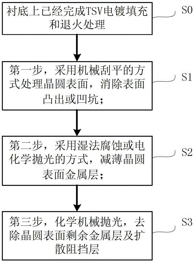
[0021] figure 1 Shown is a process flow diagram corresponding to a preferred embodiment of a TSV planarization method proposed by the present invention, and each step will be introduced below.
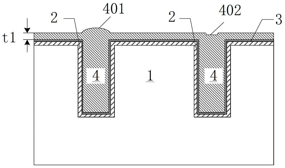
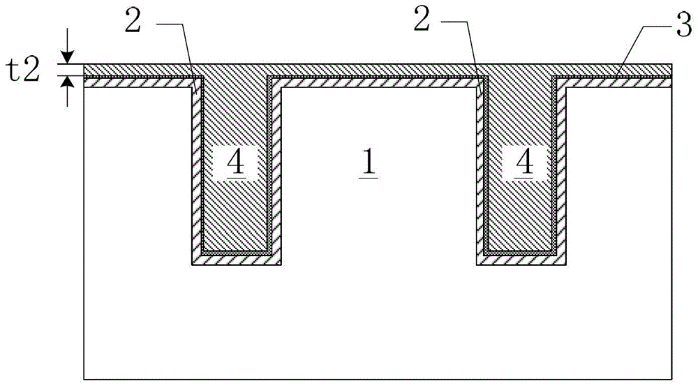
[0022] S0: if figure 2 As shown, the TSV electroplating filling and annealing operations have been completed on the wafer substrate 1 , the filling material 4 is metal copper, and the filling method is electroplating. The periphery of the TSV structure includes a sidewall insulating layer 2 and a TSV sidewall diffusion barrier layer 3 . The thickness of the copper layer on the wafer surface after electroplating and annealing treatment is t1. Subsequent TSV planarization treatment is required. Due to process defects or plating unevenness, etc., after plating and annealing, some TSV tops will have a convex or pit-like morphology, such as figure 2 There is a convex shape at ...
PUM
 Abstract
Description
Claims
Application Information


