Manufacturing method for TSV and first layer re-wiring layer with no need of CMP

A technology of rewiring layer and manufacturing method, which is applied in semiconductor/solid-state device manufacturing, electrical components, electric solid-state devices, etc., can solve the problems of high cost and many process steps, reduce process cost, reduce process steps, and eliminate CMP The effect of the polishing step

Active Publication Date: 2015-03-18
NAT CENT FOR ADVANCED PACKAGING CO LTD
View PDF3 Cites 0 Cited by
  • Summary
  • Abstract
  • Description
  • Claims
  • Application Information

AI Technical Summary

Problems solved by technology

[0009] Using this type of method, a diffusion barrier layer and a seed layer are deposited before the TSV electroplating filling. After electroplating, the surface metal layer and the diffusion barrier layer are all removed by planarization such as CMP, etc., in order to process the wiring layer. , to deposit the diffusion barrier layer and the seed layer again, so that the process steps are many and the cost is high

Method used


Image

  • Manufacturing method for TSV and first layer re-wiring layer with no need of CMP
  • Manufacturing method for TSV and first layer re-wiring layer with no need of CMP
  • Manufacturing method for TSV and first layer re-wiring layer with no need of CMP

Examples


Embodiment Construction

[0037] The present invention will be further described below in conjunction with drawings and embodiments.

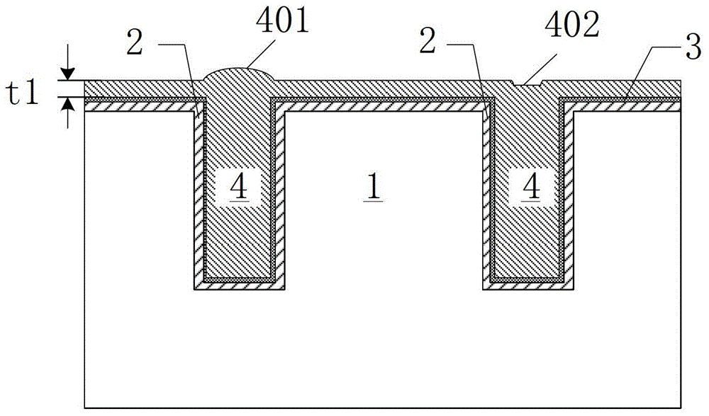
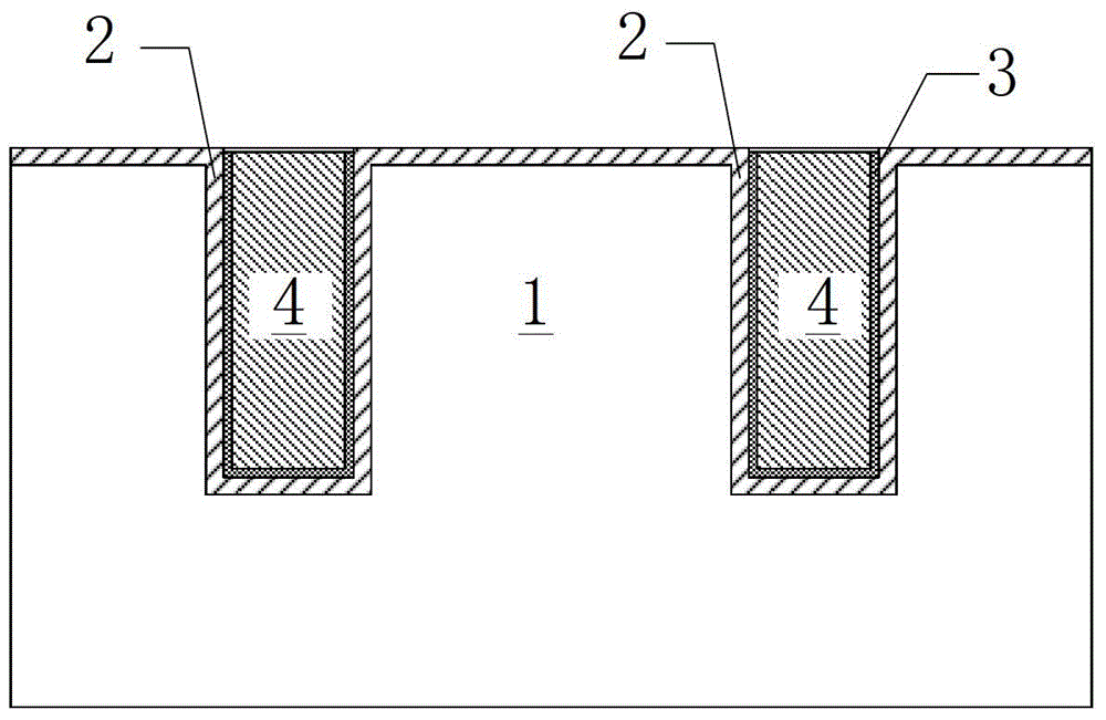
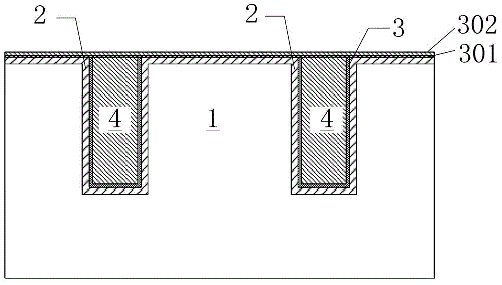
[0038] The reason why the traditional method does not reuse the diffusion barrier layer and the seed layer is that the CMP process cannot control the thickness of the remaining metal layer, and cannot guarantee that after CMP treatment, a thin layer of metal remains on the surface evenly as the seed layer for RDL electroplating. To ensure performance, the surface metal and diffusion barrier layer are generally removed, and then re-deposited. The present invention designs a special processing flow, and provides a manufacturing method of TSV and the first layer of rewiring layer without using CMP. Image 6 As shown, each process step is introduced below.

[0039] (1) S0: if Figure 7 As shown, the TSV electroplating filling and annealing operations have been completed on the substrate 1, the filling material is metal copper 4, and the filling method is electroplating. ...


PUM


Abstract

The invention provides a manufacturing method for a TSV and a first layer re-wiring layer needless of using a CMP. The method comprises the following steps of processing the surface of a substrate, eliminating the protrusions and pits on a surficial metal layer by adopting a mechanical leveling mode for the substrate being finished TSV electroplating filling, thinning the surficial metal layer of the substrate by adopting a wet etching mode or an electrochemical polishing mode, carrying out photoetching to obtain the first layer re-wiring layer, using the remained surficial metal layer of the substrate as a seed layer, and obtaining a re-wiring metal layer through electroplating, removing photoresist, and removing the surficial metal layer of the substrate and a diffusion impervious layer through corrosion to complete the manufacturing of the first layer re-wiring layer. The manufacturing method for the TSV and the first layer re-wiring layer needless of using the CMP has the advantages that after electroplating filling is carried out, the surface is processed by adopting the processing mode of mechanical leveling, then the surface copper layer is thinned, a continuous thin copper layer is remained as the electroplating seed layer of follow-up first layer RDL processing, the CMP technology is avoided, the fact that the diffusion impervious layer and the seed layer sedimentation technique are carried out once more is removed, and process cost can be lowered greatly.

Description

technical field [0001] The invention relates to a method for manufacturing a TSV and a first rewiring layer without using CMP, and belongs to the technical field of semiconductor manufacturing. Background technique [0002] Traditional TSV manufacturing includes steps such as hole etching, insulating layer deposition, diffusion barrier layer / seed layer deposition, electroplating filling, and CMP planarization, all of which require the use of expensive equipment and strict control of process quality. After TSV processing is completed, Generally, the Re-Distribution Layer (RDL) needs to be processed, which increases the cost of TSV when it is used in products. How to reduce the process cost and process difficulty and improve the yield is the core of the industrialization of TSV technology. [0003] Due to the particularity of the TSV process, after the TSV is electroplated and filled, there will be many shapes on the top of the TSV. Typical examples are: there are copper protr...

Claims


Application Information

Patent Timeline
Patent Type & Authority Patents(China)
IPC IPC(8): H01L21/768
CPCH01L21/76898H01L21/7684H01L23/481H01L2924/0002
Inventor 宋崇申张文奇顾海洋
Owner NAT CENT FOR ADVANCED PACKAGING CO LTD
Why Eureka
Try Eureka