Display device, array substrate and manufacturing method of array substrate
A technology of an array substrate and a manufacturing method, applied in the field of display devices, can solve the problems of easy disconnection, large resistance value of source-drain electrode lines, etc.
- Summary
- Abstract
- Description
- Claims
- Application Information
AI Technical Summary
Problems solved by technology
Method used
Image


Examples
Embodiment 1
[0033] In this embodiment, an array substrate is provided, and the array substrate is described by taking a bottom gate structure as an example.
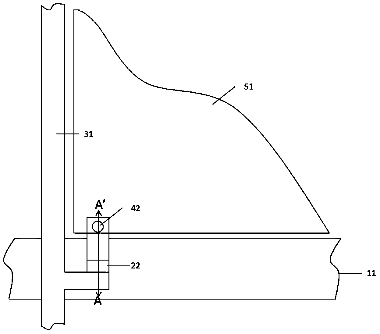
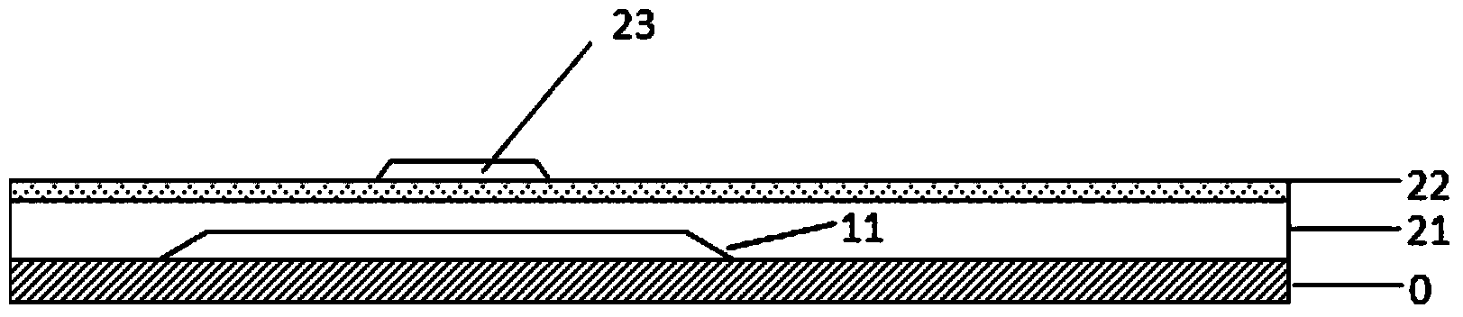
[0034] Such as figure 1 and Figure 6 As shown, the array substrate includes a substrate 0, on which a gate 11, a gate insulating layer 21, an oxide active layer, an etching stopper layer 23, a source-drain electrode layer 31, a passivation layer 41 and a pixel The electrode layer 51 ; the passivation layer 41 is provided with a via hole 42 , and the pixel electrode layer 51 is connected to the drain electrode through the via hole 42 .
[0035] The oxide active layer includes a non-metallized semiconductor region 22 and a metallized metal oxide conductor region 24;
[0036] The semiconductor region 22 corresponds to the position of the etching stopper layer 23;
[0037] The metal oxide conductor region 24 corresponds to the position of the source-drain electrode 31 and is located below the source-drain electrode 31 .
[0038] Wh...
Embodiment 2
[0041] An embodiment of the present invention provides an array substrate, which is different from Embodiment 1 in that the array substrate in this embodiment has a top-gate structure.
[0042] The array substrate may include a substrate on which a pixel electrode layer, a source-drain electrode layer, an oxide active layer, a barrier layer, a gate insulating layer and a gate are arranged, wherein the pixel electrode layer is connected to the drain electrode.
[0043] Wherein, the oxide active layer includes a semiconductor region that has not been metallized and a metal oxide conductor region that has been metallized;
[0044] The semiconductor region corresponds to the position of the etching barrier layer;
[0045] The metal oxide conductor region corresponds to the position of the source-drain electrode layer and is located above the source-drain electrode layer.
[0046] Wherein, the oxide active layer includes at least one of InGaZnO, InGaO, ITZO, and AlZnO. Of course,...
Embodiment 3
[0049] Such as Figure 7 As shown, based on the array substrate structure of Embodiment 1, the present invention also provides a method for manufacturing an array substrate, which specifically includes:
[0050] Forming the pattern of the gate on the substrate;
[0051] Specifically, refer to figure 2 , deposit a gate metal film on the substrate 0, and form the pattern of the gate 11 through a patterning process. The patterning process specifically includes processes such as exposure, development, etching and stripping, and can also be a printing or screen printing process.
[0052] patterning the gate insulating layer, the oxide active layer and the etch stop layer;
[0053] Specifically, refer to image 3 1. Deposit gate insulating material, oxide semiconductor material 22 and etch stop layer material on the substrate after step 1, and form patterns of gate insulating layer 21, oxide semiconductor material and etch stop layer 23 through a patterning process.
[0054] Wh...
PUM
 Abstract
Description
Claims
Application Information
 - R&D
- Intellectual Property
- Life Sciences
- Materials
- Tech Scout
- Unparalleled Data Quality
- Higher Quality Content
- 60% Fewer Hallucinations
Browse by: Latest US Patents, China's latest patents, Technical Efficacy Thesaurus, Application Domain, Technology Topic, Popular Technical Reports.
© 2025 PatSnap. All rights reserved.Legal|Privacy policy|Modern Slavery Act Transparency Statement|Sitemap|About US| Contact US: help@patsnap.com