Thin film transistor, array substrate and display panel
A technology of thin film transistors and array substrates, applied in the display field, can solve the problems of reduced on-off ratio and increased off-state current, and achieve the effects of improving on-off ratio, reducing impedance, and reducing leakage current
- Summary
- Abstract
- Description
- Claims
- Application Information
AI Technical Summary
Problems solved by technology
Method used
Image


Examples
Embodiment Construction
[0022] The present invention will be described in detail below in conjunction with the accompanying drawings and embodiments.
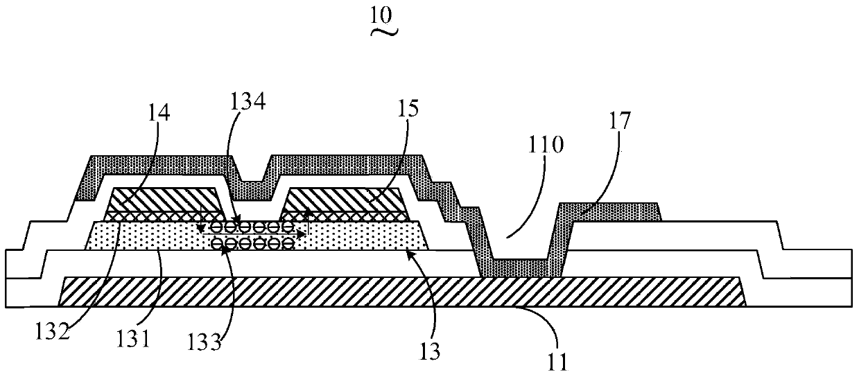
[0023] see figure 1 , figure 1 It is a structural schematic diagram of an embodiment of a thin film transistor of the present invention. Such as figure 1 As shown, the thin film transistor 10 of the present invention includes a gate 11 , a first insulating layer 12 , a semiconductor layer 13 , a source 14 , a drain 15 , a second insulating layer 16 and a conductive layer 17 . Wherein, the first insulating layer 12 is disposed on the gate 11 . The second insulating layer 16 is disposed over the first insulating layer 12 . The semiconductor layer 13 , the source electrode 14 and the drain electrode 15 are disposed between the first insulating layer 12 and the second insulating layer 16 . The conductive layer 17 is arranged on the second insulating layer 16, and is electrically connected with the gate 11, so that the thin film transistor 10 increase...
PUM
 Abstract
Description
Claims
Application Information
 - R&D
- Intellectual Property
- Life Sciences
- Materials
- Tech Scout
- Unparalleled Data Quality
- Higher Quality Content
- 60% Fewer Hallucinations
Browse by: Latest US Patents, China's latest patents, Technical Efficacy Thesaurus, Application Domain, Technology Topic, Popular Technical Reports.
© 2025 PatSnap. All rights reserved.Legal|Privacy policy|Modern Slavery Act Transparency Statement|Sitemap|About US| Contact US: help@patsnap.com