Encapsulation method for chip fan-out encapsulation structure

A packaging method and packaging structure technology, which is applied in the manufacture of electrical components, electrical solid devices, semiconductor/solid devices, etc., can solve the problems of long preparation period, difficult metal corrosion, high pollution, etc., and achieve the problem of leakage current and production cycle. The effect of environmental protection and short production cycle

Inactive Publication Date: 2014-01-01
GERAD TECH SUZHOU
View PDF3 Cites 5 Cited by
  • Summary
  • Abstract
  • Description
  • Claims
  • Application Information

AI Technical Summary

Problems solved by technology

These processes are complicated, there are many processes, and corresponding supporting fixtures are required, so the preparation period is long
[0007] 2. Waste of materials, high pollution
[0008] The development and etching process needs to remove the excess thin film dielectric layer and conductive material, resulting in a lot of material waste; a large number of chemical reagents are used in the development, electroplating or chemical crossing and corrosion processes, causing environmental pollution
[0009] 3. Leakage current problem
[0010] The metal on the thin film dielectric layer is difficult to corrode, and it is easy to cause metal residue and leakage current problem

Method used


Image

  • Encapsulation method for chip fan-out encapsulation structure
  • Encapsulation method for chip fan-out encapsulation structure
  • Encapsulation method for chip fan-out encapsulation structure

Examples


Embodiment Construction

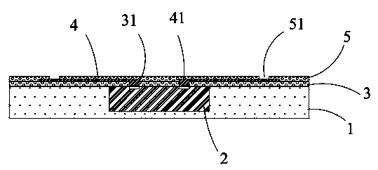
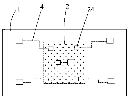
[0038] See Figures 1 to 3 The chip fan-out packaging structure in an embodiment of the present invention includes a chip 2, a plastic casing 1 encapsulated on the chip 2, a second insulating medium layer 3 arranged on the chip 2 and the plastic casing 1, and a second insulating medium layer 3 arranged on the second Several ink traces 4 on the second insulating medium layer 3 , and a first insulating medium layer 5 arranged on the ink traces 4 . The above-mentioned parts and the interrelationships between the parts will be described in detail below.

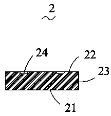
[0039] The chip 2 has a first surface 21 and a second surface 22 opposite to each other, a third surface 23 connecting the first surface 21 and the second surface 22 , and an electrode pad 24 exposed from the second surface 22 . The chip 2 can also be replaced by a combination (not shown) of a chip and passive components.

[0040] The plastic package 1 is encapsulated on the first surface 21 and the third surface 23 of the chip...


PUM


Abstract

The invention relates to an encapsulation method for a chip fan-out encapsulation structure. The encapsulation method includes the following steps that S1, a chip assembly is provided and comprises a chip and a plastic package shell encapsulated on the chip, the chip comprises a first surface, a second surface and an electrode bonding pad, the first surface and the second surface are oppositely arranged, the electrode bonding pad is exposed outwards from the second surface, the plastic package shell at least encapsulates the first surface, and the electrode bonding pad is not encapsulated by the plastic package shell; S3, a substrate ink line is formed and provided with an electrical connecting end connected with the electrode bonding pad; S4, a first thin film dielectric layer is formed, covers the substrate ink line and is provided with a first opening part enabling the substrate ink line to be partially exposed. Ink leading is adopted in the encapsulation method, so chip encapsulation is achieved. Compared with the prior art, the encapsulation method has the advantages of being simple in process, low in manufacturing cost and short in production cycle and protecting the environment, and meanwhile the problem of current leakage can be solved.

Description

technical field [0001] The invention relates to the field of semiconductor packaging, in particular to a packaging method for a chip fan-out packaging structure. Background technique [0002] The miniaturization, multi-functionalization and rapid replacement of electronic products have put forward requirements for light, thin, short, small, low-cost and flexible IC packaging, which has greatly promoted the development of advanced packaging technology. Therefore, the packaging technology for small chips, narrow-pitch multi-pin and adaptable to various packaging situations is a hot spot in the current packaging field and a future development trend. The chip fan-out packaging structure is to enlarge and arrange the narrow-pitch pins on the small chip by rewiring. This packaging structure can greatly reduce the chip size. Since chips of different designs can share the same substrate and lead frame through rewiring, more pins can be arranged as the package area increases. The e...

Claims


Application Information

Patent Timeline
Patent Type & Authority Applications(China)
IPC IPC(8): H01L21/48
CPCH01L24/81H01L24/85H01L2224/10H01L2224/42H01L21/568H01L24/19H01L2224/04105H01L2224/19H01L2924/00012
Inventor 曹凯王利明
Owner GERAD TECH SUZHOU
Why Eureka
Try Eureka