Supercharge Your Innovation With Domain-Expert AI Agents!

Solid-state imaging device

一种固体摄像元件、摄像面的技术,应用在高灵敏度化和彩色化领域,能够解决光利用率变低、增加光敏元件、入射光串扰增加等问题,达到色再现性良好、光利用率高的效果

Inactive Publication Date: 2014-01-08
PANASONIC INTELLECTUAL PROPERTY CORP OF AMERICA
View PDF8 Cites 0 Cited by
  • Summary
  • Abstract
  • Description
  • Claims
  • Application Information

AI Technical Summary

Problems solved by technology

[0021] In the prior art, if a light-absorbing color filter is used, although there is no need to greatly increase the number of photosensitive elements, there is a problem that the light utilization rate becomes low.
In addition, as in the techniques disclosed in Patent Documents 2 to 4, if dichroic mirrors and microprisms are used, light utilization efficiency can be improved, but there is a problem that photosensitive elements must be greatly increased.
[0022] On the other hand, according to the technology disclosed in Patent Document 5, although theoretically a color image with high light utilization efficiency can be surely obtained, in this technology, it is assumed that the incident light toward the imaging element is perpendicular to the imaging surface, so in practice When this technique is applied to a camera with a wide range of cameras, the occurrence of oblique light due to the amount of aperture of the lens becomes noticeable
As a result, there is a problem that the crosstalk of incident light toward each photosensitive element increases, and errors occur in color signal components.

Method used


Image

  • Solid-state imaging device
  • Solid-state imaging device
  • Solid-state imaging device

Examples


Embodiment approach 1

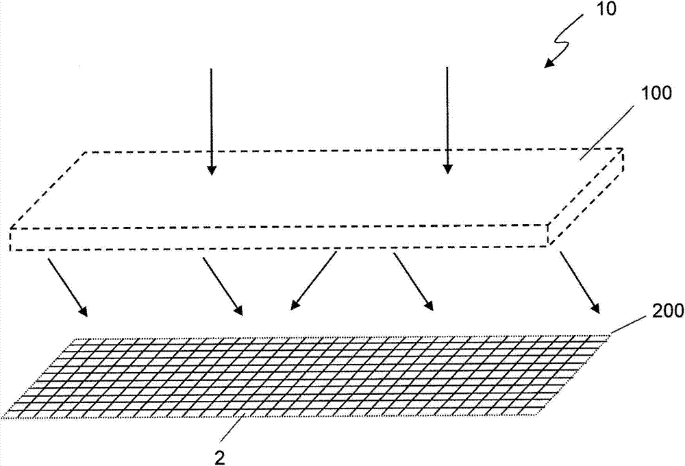
[0123] image 3 It is a block diagram showing the overall configuration of the imaging device of the first embodiment. The imaging device of this embodiment is a digital electronic camera, and includes an imaging unit 300 and a signal processing unit 400 that generates a signal (image signal) representing an image based on a signal sent from the imaging unit 300 . In addition, the imaging device may only generate still images, or may have a function of generating moving images (moving images).

[0124] The imaging section 300 is provided with the following: an optical lens 12 for imaging an object; an optical aperture 50; an optical filter 11; and the optical information imaged by the optical lens 12 and the optical filter 11 is converted into A solid-state imaging device 10 (image sensor) for electrical signals. The imaging unit 300 also includes the following: a signal generation / reception unit 13 that generates a basic signal for driving the imaging element 10 and receive...

Embodiment approach 2

[0171] Next, while referring to Figures 8A-8C , while describing the second embodiment. Compared with the imaging device of Embodiment 1, the imaging device of the present embodiment differs only in the configuration of the spectroscopic element of the imaging element 10 and signal processing, and the other components are the same. Hereinafter, differences from the imaging device of Embodiment 1 will be mainly described, and descriptions of overlapping points will be omitted.

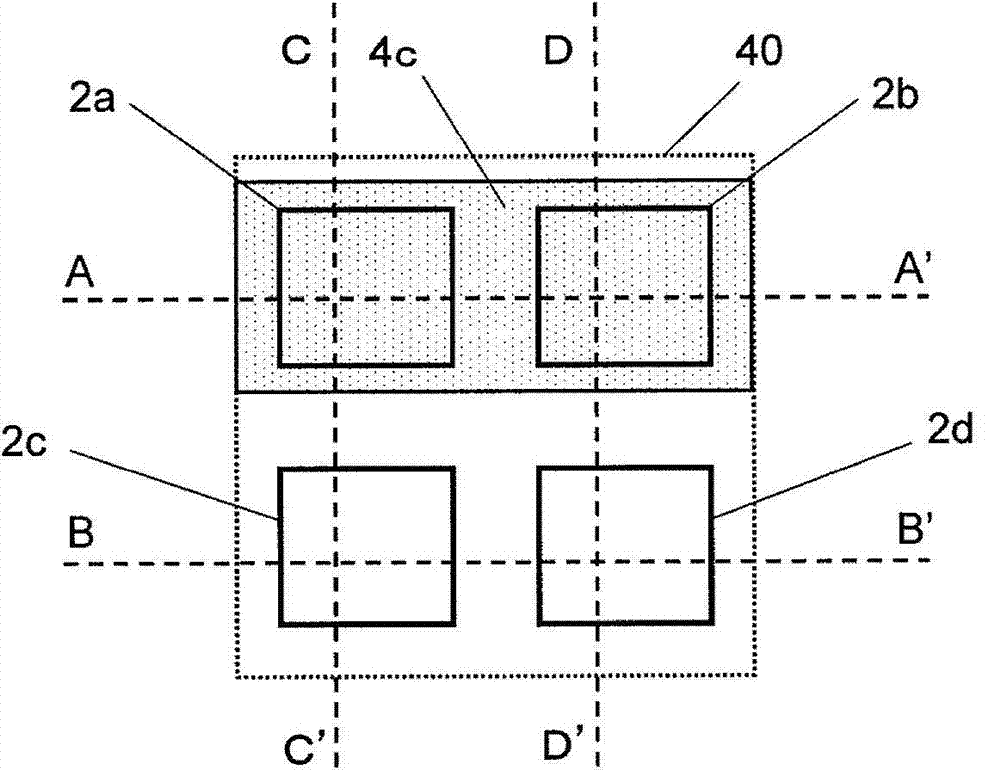
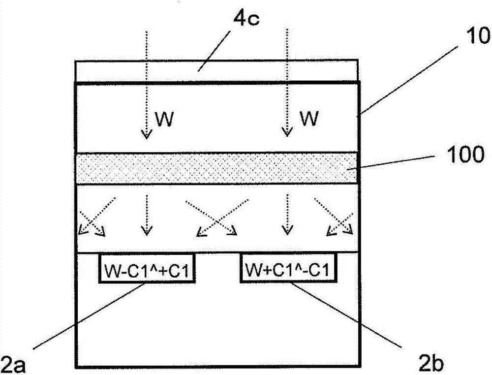
[0172] Figure 8A It is a figure which shows the basic structure of the imaging element 10 of this embodiment. Figure 8B yes Figure 8A The A-A' line profile, Figure 8C yes Figure 8A The B-B' line profile. The configuration of the spectroscopic element of the imaging element 10 of this embodiment is as follows: Figures 8A-8C As shown, in the spectroscopic element array 100, spectroscopic elements 1a for splitting light into blue light and other than blue light are arranged in the first row a...


PUM


Abstract

A solid-state imaging element is provided with a light-sensing cell array containing multiple light-sensing cells, and a spectroscopic element array containing multiple spectroscopic elements. The light-sensing cell array is configured from multiple unit blocks (40), and each unit block (40) has four light-sensing cells (2a, 2b, 2c, 2d). Moreover, a light-collecting element (4c) is disposed on a region covering light-sensing cells (2a and 2b). The light-collecting element (4c) collects the incident light onto light-sensing cells (2a and 2b).

Description

technical field [0001] The present application relates to techniques for increasing sensitivity and colorization of solid-state imaging devices. Background technique [0002] In recent years, digital cameras and digital video cameras using solid-state imaging devices such as CCDs and CMOSs ​​(hereinafter sometimes referred to as "imaging devices") have become astonishingly high in functionality and performance. In particular, the miniaturization of the pixel structure in an imaging device is progressing along with the rapid progress of semiconductor manufacturing technology. As a result, high integration of pixels and driving circuits of the imaging element can be realized, and the performance of the imaging element is promoted. In particular, in recent years, cameras using a back side illumination imaging element that receives light not on the surface (surface) side on which the wiring layer of the solid-state imaging element is formed but on the back side have also been o...

Claims


Application Information

Patent Timeline
Patent Type & Authority Applications(China)
IPC IPC(8): H01L27/14H04N9/07H04N23/12
CPCH01L27/14621H04N9/646H01L27/14629H01L27/14625H01L27/14627H04N9/045H04N9/07H04N23/84
Inventor 平本政夫藤井俊哉中村达也西胁青儿物部祐亮
Owner PANASONIC INTELLECTUAL PROPERTY CORP OF AMERICA
Features
  • R&D
  • Intellectual Property
  • Life Sciences
  • Materials
  • Tech Scout
  • Unparalleled Data Quality
  • Higher Quality Content
  • 60% Fewer Hallucinations
Learn More