Method for forming shallow trench isolation structure

A technology of isolation structures and shallow trenches, which is applied in the fields of electrical components, semiconductor/solid-state device manufacturing, circuits, etc., can solve the difficulty of process uniformity control, poor isolation performance of shallow trench isolation structures, and affect the stability of semiconductor devices, etc. problem, to achieve good isolation effect, not easy to leak, and good stability

Inactive Publication Date: 2014-01-15
SHANGHAI HUALI MICROELECTRONICS CORP
View PDF4 Cites 1 Cited by
  • Summary
  • Abstract
  • Description
  • Claims
  • Application Information

AI Technical Summary

Problems solved by technology

However, compared with the traditional high-density plasma (HDPCVD) process, although the filling capacity of the SACVD process has been greatly improved, but at the same time when this process is applied, a new integration problem arises: in the middle of the trench oxide, a a vulnerable surface (such as figure 1 As shown by the dotted circle in the middle), this fragile surface is very susceptible to erosion by the subsequent wet process, which makes it difficult to control the uniformity of the subsequent process, resulting in poor isolation performance of the shallow trench isolation structure, including the shallow trench isolation structure. Semiconductor devices are prone to leakage, which seriously affects the stability of semiconductor devices containing shallow trench isolation structures

Method used


Image

  • Method for forming shallow trench isolation structure
  • Method for forming shallow trench isolation structure
  • Method for forming shallow trench isolation structure

Examples


Embodiment Construction

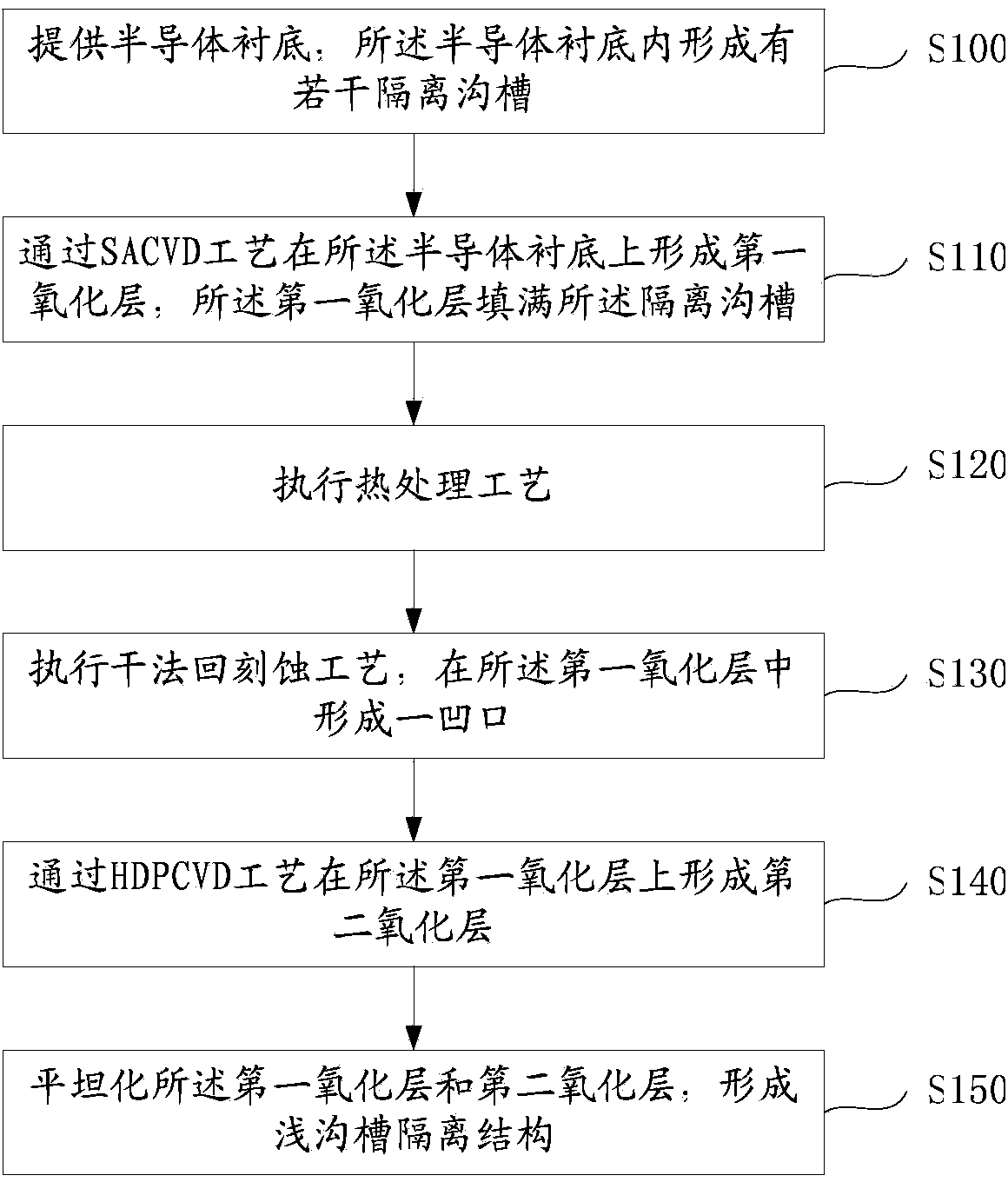
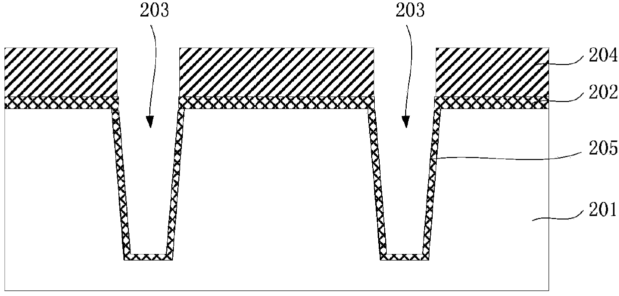
[0028] As described in the background art, with the continuous reduction of the feature size of semiconductor devices, the size of the shallow trench isolation structure used for device isolation also becomes smaller, and the aspect ratio of the isolation trench used to form the shallow trench isolation structure changes. When the oxide layer is filled in the isolation trench by the SACVD process, a fragile surface is likely to appear, resulting in poor isolation performance of the shallow trench isolation structure, and semiconductor devices including the shallow trench isolation structure are prone to leakage and poor stability. Therefore, in the present invention, after the first oxide layer is formed by the SACVD process, a dry etch-back process is performed to eliminate the fragile surface in the first oxide layer, and then the second oxide layer is formed by the HDPCVD process. In addition, a heat treatment process is performed after the first oxide layer is formed by the...


PUM


Abstract

The invention provides a method for forming a shallow trench isolation structure. After a first oxidation layer is formed through an SACVD (Sub-atmospheric Chemical Vapor Deposition) process, fragile surfaces in the first oxidation layer are eliminated by carrying out a dry method back-etching process, and subsequently a second oxidation layer is formed through an HDPCVD (High Density Plasma Chemical Vapor Deposition) process. Besides, after the first oxidation layer formed through the SACVD process, a thermal treatment process is carried out, and the first oxidation layer and the second oxidation layer formed through the HDPCVD process after the thermal treatment are closely approximate to a thermal oxide in density, so that the oxides inside the trench are consistent and matched in characteristics as a whole, and no difference is caused in later procedures. Therefore, the shallow trench isolation structure formed by using the method is good in isolation effect, a semiconductor with the shallow trench isolation structure is good in stability, and electric leakage and breakdown are unlikely to happen.

Description

technical field [0001] The invention relates to the technical field of integrated circuit manufacturing, in particular to a method for forming a shallow trench isolation structure. Background technique [0002] As the semiconductor technology enters the deep sub-micron era, most components below 0.18 microns (such as between the active regions of CMOS integrated circuits) are mostly fabricated using shallow trench isolation (STI) for lateral isolation. With the continuous reduction of the feature size of the semiconductor device, the size of the shallow trench isolation structure used for device isolation also becomes smaller, and correspondingly, the aspect ratio of the isolation trench used to form the shallow trench isolation structure becomes larger. [0003] In the existing advanced manufacturing process, starting from the 45nm technology node, its shallow trench isolation process has begun to use sub-atmospheric pressure chemical vapor deposition (SACVD) process for tr...

Claims


Application Information

Patent Timeline
Patent Type & Authority Applications(China)
IPC IPC(8): H01L21/762
CPCH01L21/76224
Inventor 郑春生张文广陈玉文
Owner SHANGHAI HUALI MICROELECTRONICS CORP
Why Eureka
Try Eureka