However, this physical scaling of device sizes raises significant issues, especially in connection with embedded SRAM and in SRAM realized as “stand-alone” memory
integrated circuit devices.
Several of these issues are due to increased variability in the electrical characteristics of transistors formed at these extremely small feature sizes.
This variability in characteristics has been observed to increase the likelihood of read and write functional failures, on a cell-to-cell basis.
The combination of increased device variability with the larger number of memory cells (and thus transistors) within an
integrated circuit renders a
high likelihood that one or more cells cannot be read or written as expected.
As mentioned above, device variability can cause read and write failures, particularly in memory cells constructed with sub-micron minimum feature size transistors.
A write failure occurs when an addressed
SRAM cell does not change its stored state when written with the opposite data state.
Typically, this failure has been observed to be due to the inability of write circuitry to pull down the storage node currently latched to a
high voltage.
Cell stability failures are the converse of write failures—a write failure occurs if a cell is too stubborn in changing its state, while a cell stability failure occurs if a cell changes its state too easily.
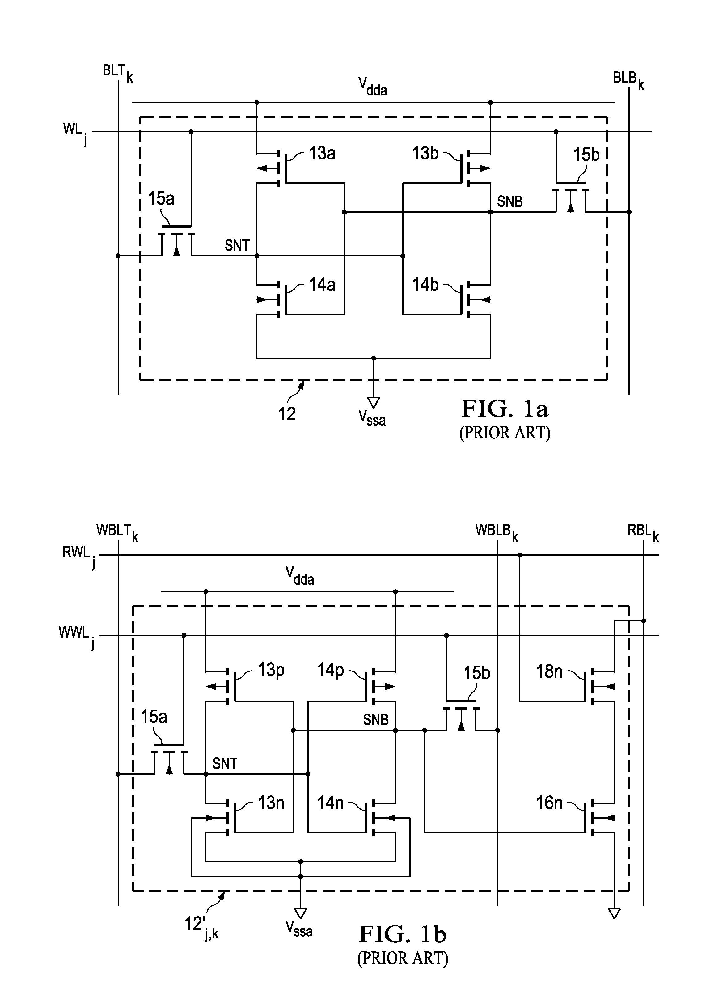
However, both the conventional 6-
T cell of FIG. 1a and the conventional 8-
T cell of FIG. 1b are vulnerable to unintentional change of state during the writing of data to other cells.
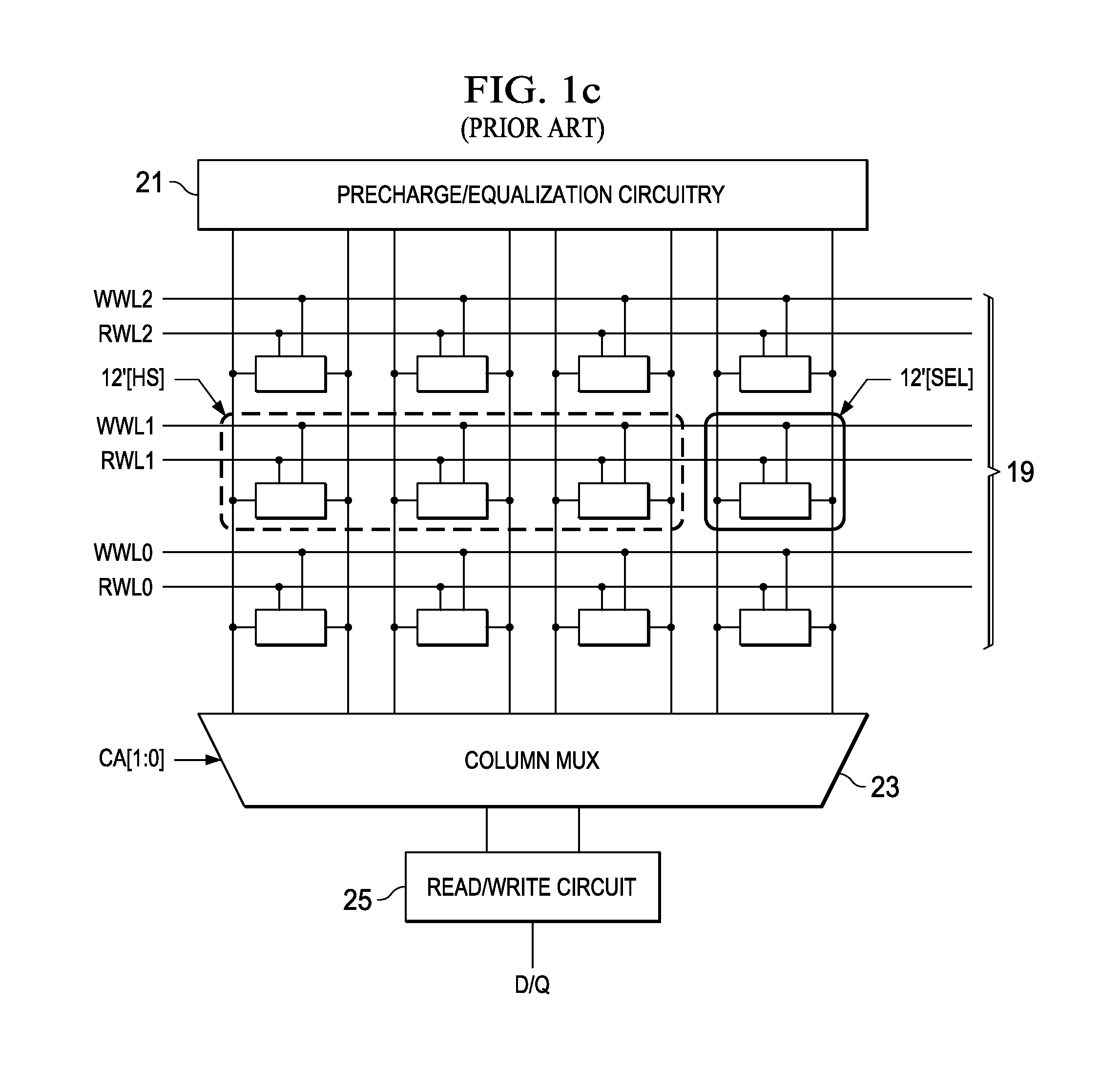
More specifically, it has been observed that SRAM cells in unselected columns of selected rows (i.e., “half-selected” cells) are especially vulnerable to the “disturb” condition present on their bit lines during writes to cells in the same row.
This effect can upset the stored data state, particularly for half-selected cells in which the transistors are imbalanced due to process variations.
In addition,
noise of sufficient magnitude
coupling to the bit lines of the half-selected columns, during a write to the selected columns in the same row, can cause a false write of data to those half-selected columns.
The possibility of such stability failure is exacerbated by device mismatch and variability, as discussed above.
Unfortunately, the design window in which both adequate cell stability and adequate
write margin can be attained is becoming smaller with continued scaling-down of device feature sizes, for the reasons mentioned above.
In addition, it has been observed that the relative drive capability of p-channel MOS transistors relative to re-channel MOS transistors is increasing as device feature sizes continue to shrink, which skews the design window toward cell stability over
write margin.
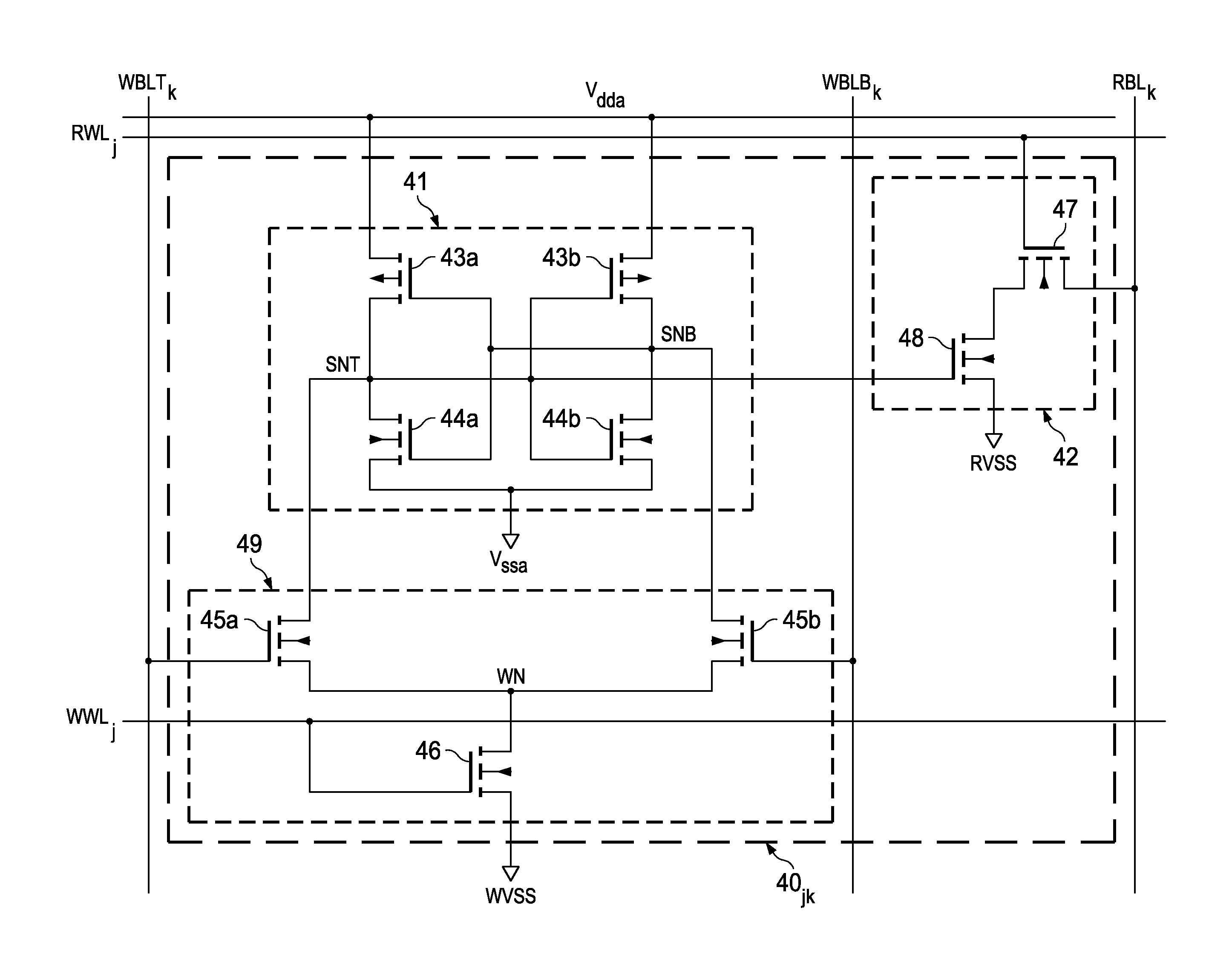
However, because pass transistors 15a, 15b are turned on for unselected columns in selected row j, cell 12″j,k also suffers from the cell stability, or disturb
vulnerability, described above.
The isolation gate, when turned off, eliminates modulation at one of the storage nodes from affecting the state of the opposite
inverter, breaking the
feedback loop for
bit line noise and inhibiting stability failures.
In addition, the asymmetric
layout of the 7-
T cell precludes implementation in an interleaved array architecture, increasing the likelihood of multiple-bit soft errors, and further reducing
chip area efficiency.
