

Chip structure and manufacturing method thereof
A technology of chip structure and manufacturing method, which is applied in semiconductor/solid-state device manufacturing, semiconductor devices, electrical components, etc., and can solve the problems of large chip terminal width, low terminal utilization rate, and limited chip withstand voltage capability.
- Summary
- Abstract
- Description
- Claims
- Application Information
AI Technical Summary
Problems solved by technology
Method used
Image

Examples
Embodiment Construction
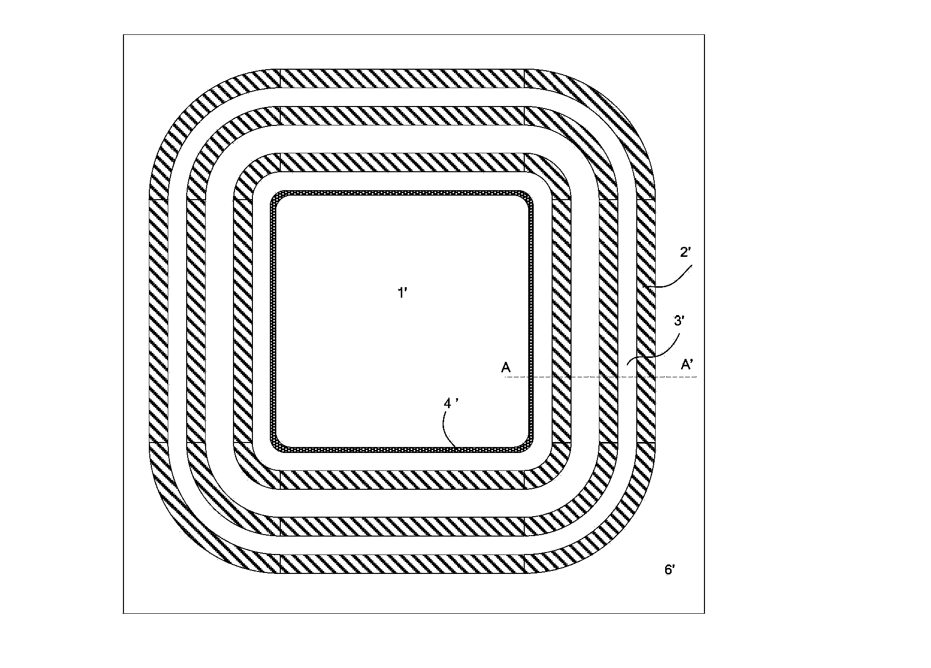
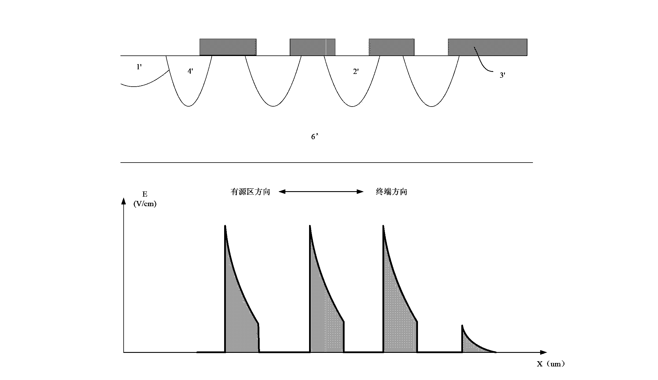
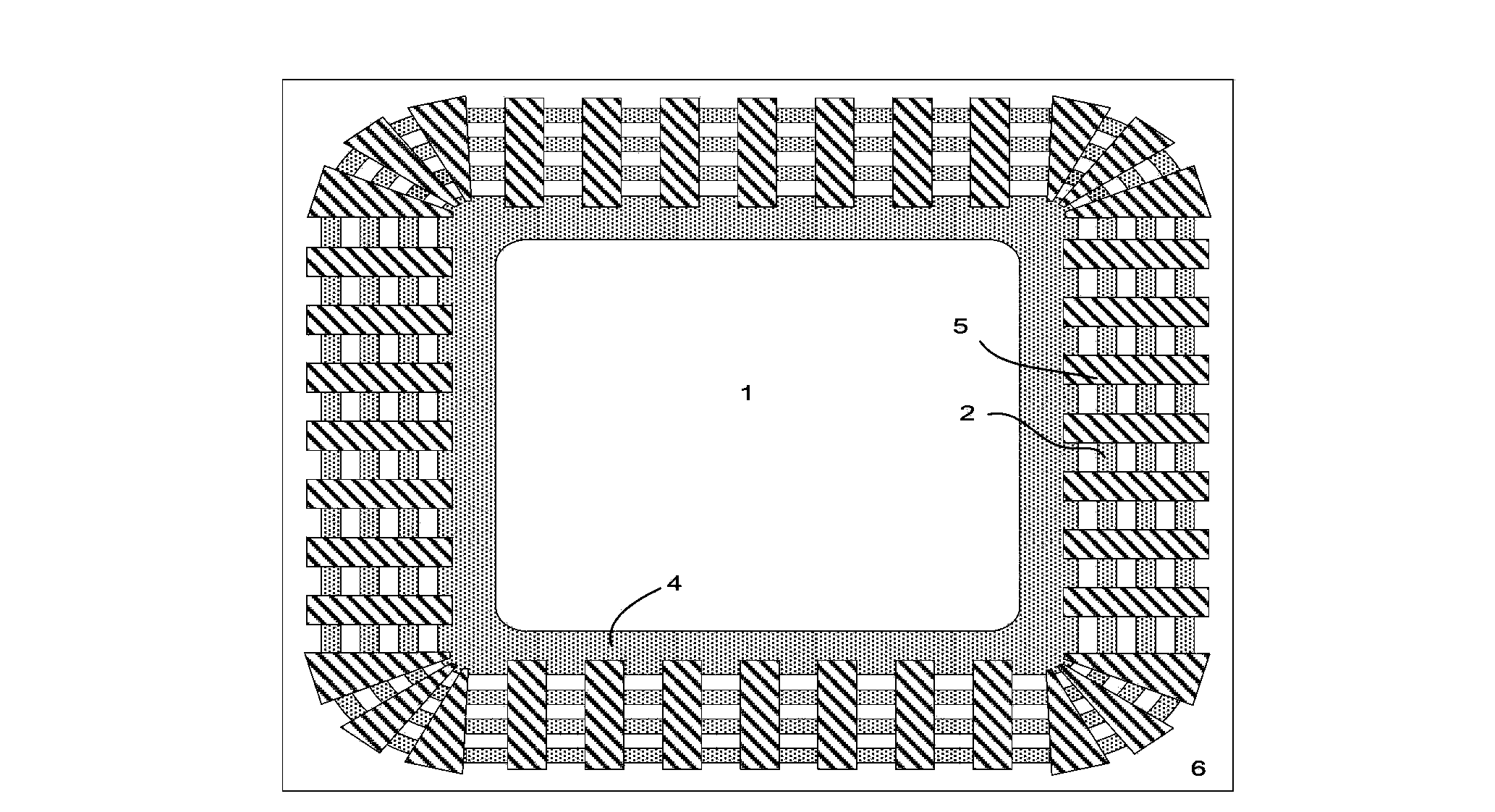
[0033] The embodiments of the present invention are described in detail below. Examples of the embodiments are shown in the accompanying drawings, in which the same or similar reference numerals indicate the same or similar elements or elements with the same or similar functions. The embodiments described below with reference to the accompanying drawings are exemplary, and are only used to explain the present invention, and cannot be construed as limiting the present invention.
[0034] In the description of the present invention, it should be understood that the terms "center", "longitudinal", "transverse", "upper", "lower", "front", "rear", "left", "right", " The orientation or positional relationship indicated by "vertical", "horizontal", "top", "bottom", "inner", "outer", etc. are based on the orientation or positional relationship shown in the drawings, and are only for the convenience of describing the present invention and simplifying The description does not indicate or i...
PUM
 Abstract
Description
Claims
Application Information