A Schottky semiconductor device with charge compensation trench and its preparation method

A charge compensation, conductive semiconductor technology, used in semiconductor/solid-state device manufacturing, semiconductor devices, circuits, etc., can solve problems such as fast turn-on and turn-off, low forward turn-on voltage, and impact on reverse breakdown characteristics of devices. The effect of reducing forward conduction resistance, increasing impurity doping concentration, and improving forward conduction characteristics

Active Publication Date: 2017-08-08
北海惠科半导体科技有限公司
View PDF4 Cites 0 Cited by
  • Summary
  • Abstract
  • Description
  • Claims
  • Application Information

AI Technical Summary

Problems solved by technology

[0002] Power semiconductor devices are widely used in power management and power applications, especially semiconductor devices involving Schottky junctions have become an important trend in device development. Schottky devices have the advantages of low forward turn-on voltage and fast turn-on and turn-off speed. At the same time, Schottky devices also have the disadvantages of large reverse leakage current and cannot be used in high-voltage environments.
[0003] Schottky diodes can be manufactured through a variety of different layout techniques, the most commonly used is planar layout, the traditional planar Schottky diode has a sudden electric field distribution curve in the drift region, which affects the reverse breakdown characteristics of the device, while the traditional The planar Schottky diode has a high on-resistance

Method used


Image

  • A Schottky semiconductor device with charge compensation trench and its preparation method
  • A Schottky semiconductor device with charge compensation trench and its preparation method
  • A Schottky semiconductor device with charge compensation trench and its preparation method

Examples


Embodiment 1

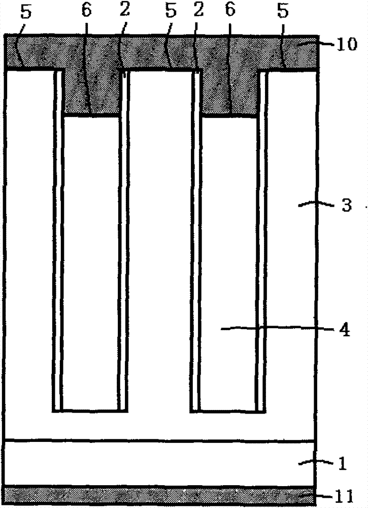
[0026] figure 1 It is a cross-sectional view of a Schottky semiconductor device with a charge compensation trench of the present invention, combined below figure 1 The semiconductor device of the present invention will be described in detail.

[0027] A Schottky semiconductor device with a charge compensation trench, comprising: a substrate layer 1, which is an N conductivity type semiconductor silicon material, and the doping concentration of phosphorus atoms is 1E19 / CM 3 , on the lower surface of the substrate layer 1, the electrodes are drawn out through the lower surface metal layer 11; the first conductive semiconductor material 3, located on the substrate layer 1, is a semiconductor silicon material of N conductivity type, and the doping concentration of phosphorus atoms is 1E16 / CM 3 ; The second conductive semiconductor material 4, located in the first conductive semiconductor material 3, is a semiconductor silicon material of P conductivity type, and the doping concen...

Embodiment 2

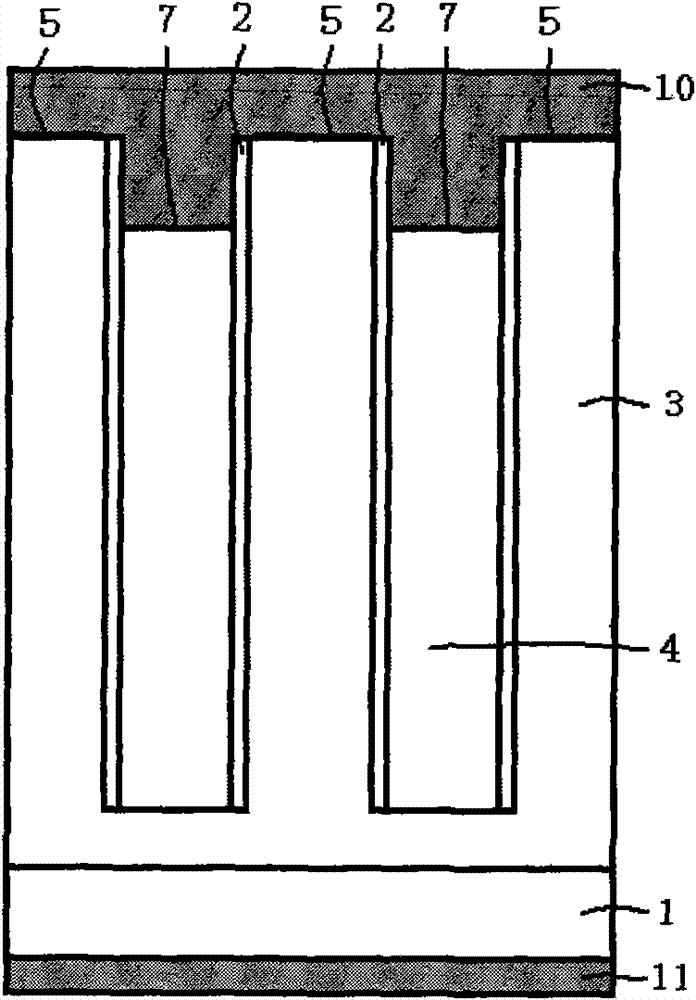
[0040] Figure 6 It is a cross-sectional view of a Schottky semiconductor device with a charge compensation trench of the present invention, combined below Figure 6 The semiconductor device of the present invention will be described in detail.

[0041] A Schottky semiconductor device with a charge compensation trench, comprising: a substrate layer 1, which is an N conductivity type semiconductor silicon material, and the doping concentration of phosphorus atoms is 1E19 / CM 3 , on the lower surface of the substrate layer 1, the electrodes are drawn out through the lower surface metal layer 11; the second conductive semiconductor material 4, located on the substrate layer 1, is a semiconductor silicon material of P conductivity type, and the doping concentration of boron atoms is 1E16 / CM 3 ; The first conductive semiconductor material 3, located in the second conductive semiconductor material 4, is a semiconductor silicon material of N conductivity type, and the doping concentr...


PUM


Abstract

The invention discloses a Schottky semiconductor device with a charge compensation groove. According to the Schottky semiconductor device with the charge compensation groove, a charge compensation structure can be formed by a first conductive semiconductor material and a second conductive semiconductor material, electric field intensity which can reduce Schottky junctions on the surface of the first conductive semiconductor material exists in the groove in the surface of the device, and then reverse breakdown voltage of the device is improved. The invention further provides a preparing method of the Schottky semiconductor device with the charge compensation groove.

Description

technical field [0001] The invention relates to a Schottky semiconductor device with a charge compensation trench, and also relates to a preparation method of the Schottky semiconductor device with a partial charge compensation trench. The semiconductor device of the present invention is a basic structure for manufacturing power rectifying devices. Background technique [0002] Power semiconductor devices are widely used in power management and power applications, especially semiconductor devices involving Schottky junctions have become an important trend in device development. Schottky devices have the advantages of low forward turn-on voltage and fast turn-on and turn-off speed. At the same time, Schottky devices also have disadvantages such as large reverse leakage current and cannot be used in high-voltage environments. [0003] Schottky diodes can be manufactured through a variety of different layout techniques, the most commonly used is planar layout, the traditional ...

Claims


Application Information

Patent Timeline
Patent Type & Authority Patents(China)
IPC IPC(8): H01L29/872H01L29/06H01L21/329
CPCH01L29/0684H01L29/66143H01L29/872
Inventor 朱江
Owner 北海惠科半导体科技有限公司
Why Eureka
Try Eureka