Method for preventing wire cutting steel wires from being broken and improving silicon wafer yield

A technology for cutting steel wire and silicon rod yield rate, which is applied to fine working devices, stone processing equipment, manufacturing tools, etc. Line defects, preventing splits, and ensuring the effect of chip yield

Inactive Publication Date: 2014-01-22
JIANGSU ZHAOJING PHOTOELECTRIC TECH DEV
View PDF0 Cites 4 Cited by
  • Summary
  • Abstract
  • Description
  • Claims
  • Application Information

AI Technical Summary

Problems solved by technology

During the processing, when the silicon wafers located at both ends of the sub-ingot are at the beginning of cutting or near the end of cutting, they are prone to chipping, missing corners, and chipped edges due to the impact of mortar. The slope at a certain angle leads to uneven thickness of the silicon wafers located at both ends of the sub-ingot. During the cutting process, due to the uneven thickness of the silicon wafers, the steel wire is stressed unevenly. Therefore, it is easy to cause the cutting steel wire to break when cutting here Even if the cutting wire is not broken, the damage rate of the silicon wafers at both ends is relatively high. Usually, more than 10 defective silicon wafers are produced for each cut, which not only affects the yield of silicon rods, but also affects the cutting quality of the cut silicon wafers. , increased downtime wiring time at the same time, will all be scrapped for cutting the whole roll of steel wire for high-quality silicon wafers, if vertical glass plates 4 are not added at the exposed ends of the sub-ingot silicon rods 1, the number of defective silicon wafers produced by each cutting will decrease bigger

Method used


Image

  • Method for preventing wire cutting steel wires from being broken and improving silicon wafer yield
  • Method for preventing wire cutting steel wires from being broken and improving silicon wafer yield
  • Method for preventing wire cutting steel wires from being broken and improving silicon wafer yield

Examples


Embodiment 1

[0017] Embodiment 1: a kind of method that prevents the cutting steel wire from breaking and improves the yield of silicon rods,

[0018] The first step, cutting of square sub-ingots: cutting the polysilicon ingots into square sub-ingots;

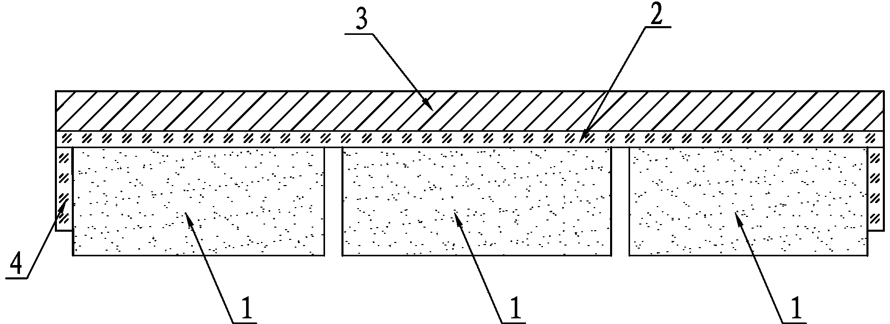
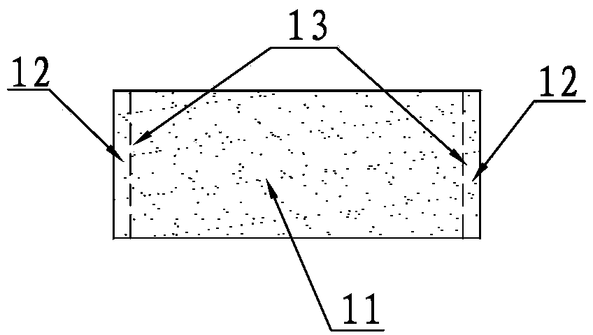
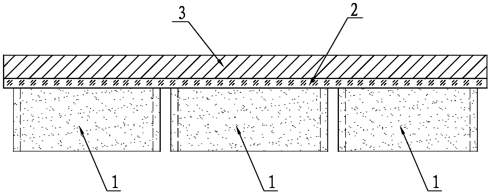
[0019] The second step is to cut the silicon ingot to be sliced: the square sub-ingot obtained in the first step is subjected to the minority carrier lifetime test, and the silicon wafer cutting section 11 and the silicon wafers located at both ends of the silicon wafer cutting section are determined according to the minority carrier lifetime parameter. Invalid section of the rod, and marking line 13 is marked at the boundary. When cutting off the invalid section of the silicon rod at both ends, a process protection section 12 of 2 to 5 mm is reserved at both ends of the silicon wafer cutting section 11. After cutting Obtain the sub-ingot silicon rod 1 with the process protection end, the sub-ingot silicon rod 1 with the process protection ...


PUM


Abstract

The invention discloses a method for preventing wire cutting steel wires from being broken and improving the silicon wafer yield. The method includes the steps of sub-ingot-blank cutting, sub-ingot-silicon-rod cutting, sub-ingot-silicon-rod bonding and cutting steel wire distribution cutting, wherein each sub-ingot-silicon-rod is composed of a silicon wafer cutting section and process protection sections, and the process protection sections are arranged at the two ends of the silicon wafer cutting sections. When the cutting steel wires are distributed, it is guaranteed that the two steel wires, located on the outer sides, in each set of cutting steel wires are located inside the corresponding silicon wafer cutting section. Due to the fact that the process protection sections are reserved at the two ends of the sub-ingot-silicon-rods to be cut, in the silicon wafer cutting process, the process protection sections located at the two ends of the sub-ingot-silicon-rods have the protection effect on silicon wafers at the outmost ends, the defects of breakage, unfilled corners, edge breakage and the like of the silicon wafers can be prevented, the silicon wafer yield and the silicon wafer pass percent are improved, and the defect that the steel wires are broken due to uneven stress can also be effectively prevented.

Description

Technical field: [0001] The invention relates to the wire-cutting technology of polycrystalline silicon wafers, in particular to a method for preventing wire-cutting steel wires of silicon wafers from breaking and improving the qualified rate and yield of silicon wafers. technical background: [0002] Solar polysilicon wafers are the most basic raw materials for solar cells. The existing production method of polysilicon wafer is multi-wire cutting. Before processing polycrystalline silicon wafers, the silicon ingot is first cut into squares to obtain a sub-ingot with a square cross section, and then the minority carrier life of the square sub-ingot is tested, and the part with a low minority carrier life at both ends of the square sub-ingot (that is, the invalid length part) ) to obtain sub-ingot silicon rods, and finally bond the sub-ingot silicon rods to the workpiece plate. The bonding structure is as follows figure 1 As shown, the sub-ingot silicon rod 1 is bonded on t...

Claims


Application Information

Patent Timeline
Patent Type & Authority Applications(China)
IPC IPC(8): B28D5/04
Inventor 杨方谈军王庆峰丁海军陈远峰
Owner JIANGSU ZHAOJING PHOTOELECTRIC TECH DEV
Why Eureka
Try Eureka