3C-SiC epitaxial structure

An epitaxial structure, 3c-sic technology, applied in the direction of semiconductor devices, electrical components, circuits, etc., can solve the problems of poor bonding force between the film and the substrate, poor adhesion, unfavorable 3C-SiC nucleation and growth, etc., to achieve inhibition Interfacial void defects, improving the withstand voltage performance, and alleviating the effects of lattice mismatch

Pending Publication Date: 2020-08-28
安徽长飞先进半导体有限公司
View PDF0 Cites 0 Cited by
  • Summary
  • Abstract
  • Description
  • Claims
  • Application Information

AI Technical Summary

Problems solved by technology

However, when 3C-SiC is epitaxially grown on a Si substrate, the Si atoms on the substrate surface diffuse outward under high temperature conditions to form vacancies, and these vacancies are combined to form larger cavities. When the carbon source and silicon source are introduced, the direct Films are grown on the surface of hollow substrates, and these interfacial voids deteriorate the bonding force between the film and the substrate and affect the epitaxial growth of 3C-SiC films
At the same time, the interface state density of 3C-SiC grown on the Si substrate is high, and there is a 20% lattice mismatch and 8% thermal expansion mismatch between the Si substrate and the 3C-SiC film, which hinders the 3C-SiC device. development of
[0005] However, the epitaxial growth of 3C-SiC on the sapphire substrate is not conducive to the initial nucleation and growth of 3C-SiC due to its poor adhesion to silicon carbide.

Method used


Image

  • 3C-SiC epitaxial structure
  • 3C-SiC epitaxial structure
  • 3C-SiC epitaxial structure

Examples


Embodiment 1

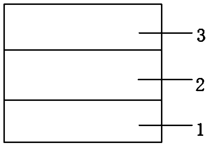
[0041] A 3C-SiC epitaxial structure, the 3C-SiC epitaxial structure includes a substrate 1, a GaN buffer layer 2, and a 3C-SiC epitaxial layer 3 sequentially from bottom to top.

[0042] The preparation method of the 3C-SiC epitaxial structure comprises the following steps:

[0043] 1) Putting the substrate into the reaction chamber of the CVD system, and evacuating the reaction chamber; the substrate is a sapphire substrate;

[0044] 2) Growth of GaN buffer layer: Carrier gas H is introduced at flow rates of 10-50slm, 50-100sccm and 80-200sccm respectively 2 , TMGa and NH 3 , growing a GaN layer with a thickness of 10-500nm at a temperature of 1000-1250°C and a pressure of 100-500mbar;

[0045] 3) Growth of 3C-SiC epitaxial layer: Introduce H at flow rates of 10-50slm, 100-500sccm, 100-500sccm, 80-150sccm and 15-50sccm respectively 2 , silicon source, carbon source and N 2 , growing an epitaxial layer with a thickness of 10-100 μm at a temperature of 1200-1450 ° C and a pre...

Embodiment 2

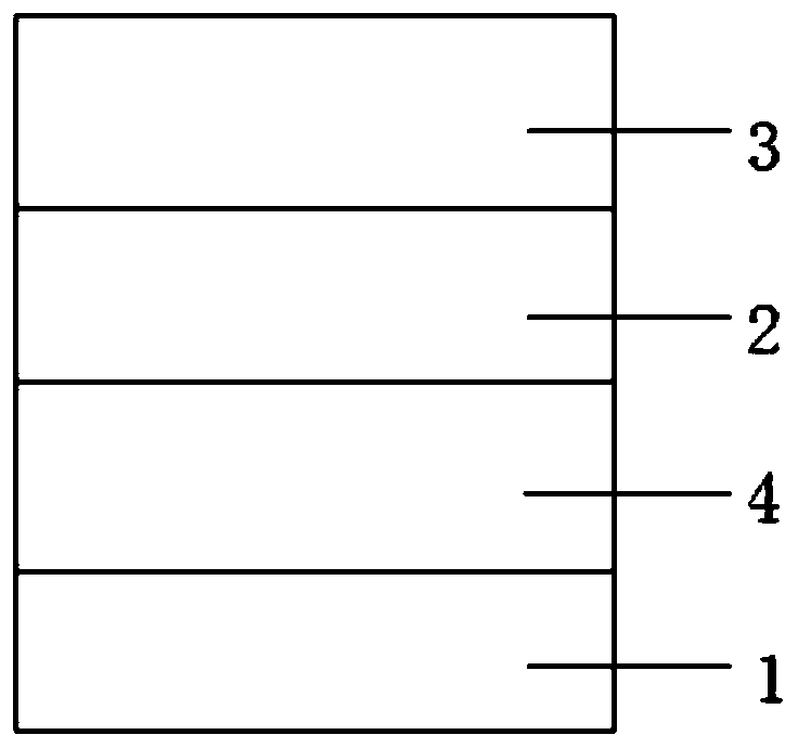
[0048] A 3C-SiC epitaxial structure, the 3C-SiC epitaxial structure sequentially includes a substrate, an AlGaN buffer layer 4, a GaN buffer layer 2, and a 3C-SiC epitaxial layer 3 from bottom to top.

[0049] The preparation method of the 3C-SiC epitaxial structure comprises the following steps:

[0050] 1) Putting the substrate into the reaction chamber of the CVD system, and evacuating the reaction chamber; the substrate is a sapphire substrate;

[0051] 2) Growth of AlGaN buffer layer: the carrier gas H is passed through at the flow rates of 10-50slm, 50-100sccm, 50-100sccm and 80-200sccm respectively 2 , TMGa, TMAl and NH 3 , growing an AlGaN layer with a thickness of 10-500nm and an Al composition of 10-40% at a temperature of 1000-1250°C and a pressure of 100-500mbar;

[0052] 3) Growth of GaN buffer layer: Carrier gas H is introduced at flow rates of 10-50slm, 50-100sccm and 80-200sccm respectively 2 , TMGa and NH 3 , growing a GaN layer with a thickness of 10-500n...

Embodiment 3

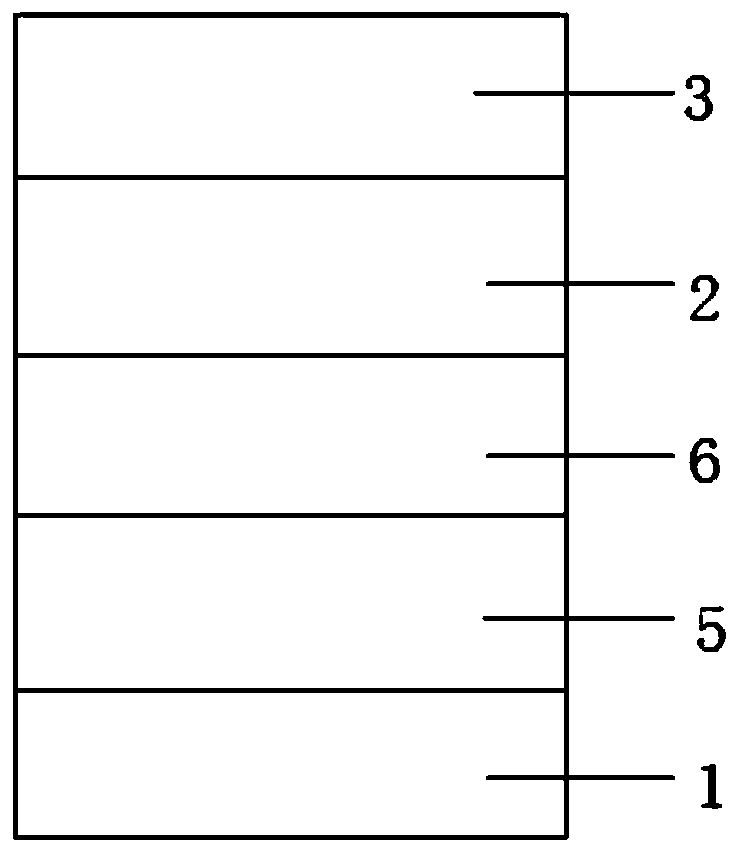
[0056] A 3C-SiC epitaxial structure, the 3C-SiC epitaxial structure sequentially includes a substrate 1, an AlGaN buffer layer A5, an AlGaN buffer layer B6, a GaN buffer layer 2, and a 3C-SiC epitaxial layer 3 from bottom to top.

[0057] The preparation method of the 3C-SiC epitaxial structure comprises the following steps:

[0058] 1) Put the substrate into the reaction chamber of the CVD system, and evacuate the reaction chamber; the substrate is a sapphire substrate;

[0059] 2) Growth of AlGaN buffer layer A: Pass carrier gas H at flow rates of 10-50slm, 50-100sccm, 50-100sccm and 80-200sccm respectively 2 , TMGa, TMAl and NH 3 , growing an AlGaN layer with a thickness of 10-500nm and an Al composition of 30-40% at a temperature of 1000-1250°C and a pressure of 100-500mbar;

[0060] 3) Growth of the AlGaN buffer layer B: flow the carrier gas H at the flow rates of 10-50slm, 50-100sccm, 50-100sccm and 80-200sccm respectively 2 , TMGa, TMAl and NH 3 , growing an AlGaN l...


PUM

PropertyMeasurementUnit
thicknessaaaaaaaaaa
thicknessaaaaaaaaaa
thicknessaaaaaaaaaa

Abstract

The invention discloses a 3C-SiC epitaxial structure. The 3C-SiC epitaxial structure sequentially comprises a substrate, a GaN buffer layer and a 3C-SiC epitaxial layer from bottom to top. The GaN buffer layer with higher forbidden band width and critical breakdown field intensity is inserted between the substrate and the 3C-SiC epitaxial layer, so that the voltage withstanding performance of the3C-SiC device is improved. When the 3C-SiC grows on the Si substrate, the diffusion of Si atoms during the heating process will form interface holes, an AlN buffer layer grows on the Si substrate firstly, and atom migration recrystallization hardly occurs once the AlN buffer layer covers the substrate at a high temperature, so that the defect of the interface holes formed by volatilization of Si is effectively inhibited, and a high-quality 3C-SiC epitaxial structure is obtained.

Description

technical field [0001] The invention belongs to the technical field of semiconductors, and in particular relates to a 3C-SiC epitaxial structure. Background technique [0002] The third-generation wide bandgap semiconductor materials represented by SiC materials have the characteristics of wide bandgap, high critical breakdown electric field, high thermal conductivity, high carrier saturation drift, etc., and are especially suitable for making high temperature, high pressure, high frequency, high power, anti- Irradiation and other semiconductor devices. [0003] Among SiC polytypes, crystal forms such as 3C-SiC, 4H-SiC, and 6H-SiC are the most widely used. Compared with other crystal forms, 3C-SiC has higher saturation electron drift rate, electron mobility and hole mobility. High, making 3C-SiC more potential in high-frequency device applications. However, the band gap and critical breakdown field strength of 3C-SiC are low, which restricts the application of 3C-SiC in hi...

Claims


Application Information

Patent Timeline
Patent Type & Authority Applications(China)
IPC IPC(8): H01L29/06
CPCH01L29/0611H01L29/0615H01L29/0684
Inventor 左万胜钮应喜刘洋张晓洪刘锦锦袁松史田超史文华钟敏
Owner 安徽长飞先进半导体有限公司
Why Eureka
Try Eureka