
Etching method for silicon oxide and silicon nitride double-layer composite side wall (ON side wall)

A technology of silicon oxide and silicon nitride, which is applied in the direction of semiconductor devices, electrical components, circuits, etc., can solve the problem of unfavorable control of the bottom side wall width, and achieve the effect of avoiding damage and controlling the gate width

Active Publication Date: 2014-01-22
锐立平芯微电子(广州)有限责任公司
View PDF5 Cites 2 Cited by
  • Summary
  • Abstract
  • Description
  • Claims
  • Application Information

AI Technical Summary

Problems solved by technology

Based on this, after the ON sidewall etching is completed, it is easy to form a slope structure, such as figure 1 The cross-sectional view of the ON sidewall morphology formed by the traditional method, in which the ON sidewalls on both sides are oblique structures, which is unfavorable for the control of the width of the bottom sidewall

Method used


Image

  • Etching method for silicon oxide and silicon nitride double-layer composite side wall (ON side wall)
  • Etching method for silicon oxide and silicon nitride double-layer composite side wall (ON side wall)
  • Etching method for silicon oxide and silicon nitride double-layer composite side wall (ON side wall)

Examples


Embodiment Construction

[0019] The present invention will be described in detail below in conjunction with the accompanying drawings and by taking specific implementations as examples. However, those skilled in the art should know that the present invention is not limited to the specific embodiments listed, as long as it conforms to the spirit of the present invention, it should be included in the protection scope of the present invention.

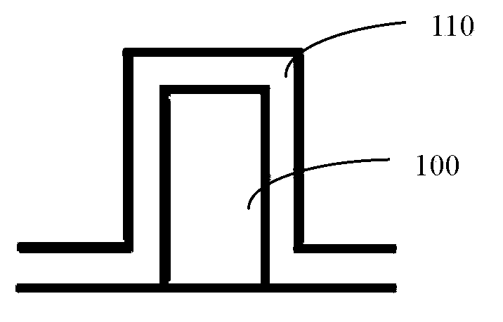
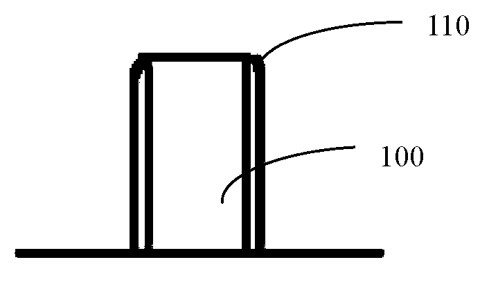
[0020] The etching method of the silicon oxide and silicon nitride double-layer composite sidewall of the present invention divides the etching of the ON sidewall into two steps of main etching and over-etching. The main etching step is not triggered to stop when it touches silicon oxide, but stops when 2 / 3 to 4 / 5 of the silicon nitride thickness is etched away, and then switches to the over-etching step, which is convenient for controlling the ON sidewall The main function of the over-etching step is to etch the remaining silicon nitride thickness and stop on th...


PUM


Abstract

The invention discloses an etching method for a silicon oxide and silicon nitride double-layer composite side wall. The method comprises: first of all, sequentially depositing a silicon oxide film and a silicon nitride film after a lightly doped drain injection and a Halo process on a semiconductor device forming an offset isolation side wall; then executing a major etching step, i.e., etching the silicon nitride film to a specific thickness; executing an over-etching step, i.e., etching the residual silicon nitride film and stopping at the silicon oxide film below, and simultaneously etching clean the silicon nitride left behind on an overall wafer surface so as to form the ON side wall, the over-etching step being directly skipped to after the major etching step is finished. The major etching step enables the morphology of the ON side wall to be not too inclined to control the effective thickness of the bottom of the side wall so as to control the gate thickness of a device. The over-etching step enables the residual silicon nitride on a wafer to be etched clean through a high-selectivity menu for a silicon oxide so as to avoid the damage to a substrate.

Description

technical field [0001] The invention belongs to the field of semiconductor integrated circuit manufacturing, and more specifically relates to an etching method for a silicon oxide and silicon nitride double-layer composite side wall. Background technique [0002] In VLSI manufacturing, dielectric spacers need to be made before the lightly doped drain (LDD) implantation process to prevent source-drain implantation of a larger dose from being too close to the channel to cause source-drain breakthrough, resulting in device failure and reduced yield. [0003] The current mainstream 65nm or even 45nm sidewall manufacturing process is as follows: first deposit or thermally grow a layer of silicon dioxide film liner (Liner) on the polysilicon gate, such as using RTO to grow about 30A of silicon dioxide, as the subsequent engraving Etch barrier layer; then deposit a layer of silicon nitride film with good conformality, surrounding the polysilicon gate. Then, the silicon nitride fi...

Claims


Application Information

Patent Timeline
IPC IPC(8): H01L21/336H01L21/311
CPCH01L21/28141H01L29/66477
Inventor 孟令款
Owner 锐立平芯微电子(广州)有限责任公司
Features
  • Generate Ideas
  • Intellectual Property
  • Life Sciences
  • Materials
  • Tech Scout
  • Unparalleled Data Quality
  • Higher Quality Content
  • 60% Fewer Hallucinations
Learn More