A kind of horizontal structure trench Schottky semiconductor device and its preparation method

A horizontal structure and semiconductor technology, which is applied in semiconductor/solid-state device manufacturing, semiconductor devices, electrical components, etc., can solve the problems that cannot be applied in high-voltage environment, low forward turn-on voltage, fast turn-on and turn-off speed, etc., to improve positive Effects of conduction characteristics, high current density, and large conduction area

Active Publication Date: 2016-12-21
北海惠科半导体科技有限公司
View PDF5 Cites 0 Cited by
  • Summary
  • Abstract
  • Description
  • Claims
  • Application Information

AI Technical Summary

Problems solved by technology

[0002] Power semiconductor devices are widely used in power management and power applications, especially semiconductor devices involving Schottky junctions have become an important trend in device development. Schottky devices have the advantages of low forward turn-on voltage and fast turn-on and turn-off speed. At the same time, Schottky devices also have the disadvantages of large reverse leakage current and cannot be used in high-voltage environments.

Method used


Image

  • A kind of horizontal structure trench Schottky semiconductor device and its preparation method
  • A kind of horizontal structure trench Schottky semiconductor device and its preparation method
  • A kind of horizontal structure trench Schottky semiconductor device and its preparation method

Examples


Embodiment 1

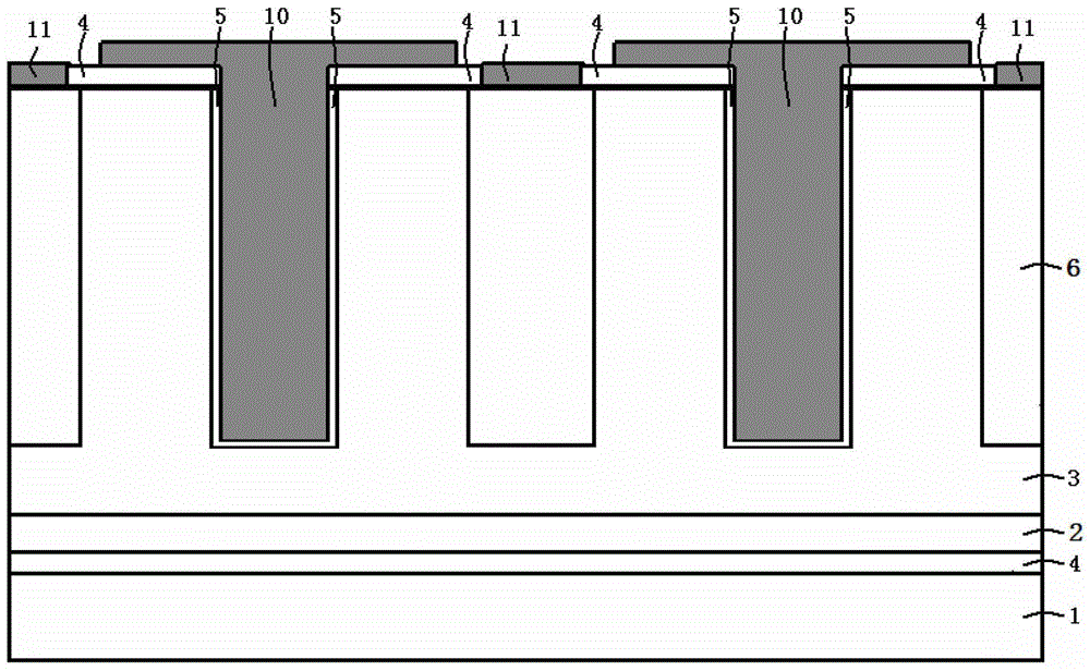
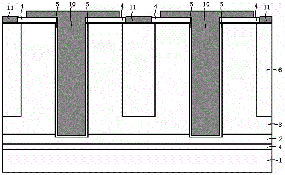
[0028] figure 1 It is a schematic cross-sectional view of a horizontal structure trench Schottky semiconductor device of the present invention, combined below figure 1 The semiconductor device of the present invention will be described in detail.

[0029] A trench Schottky semiconductor device with a horizontal structure, comprising: a substrate layer 1, which is an N conductivity type semiconductor silicon material, and the doping concentration of phosphorus atoms is 1E19 / CM 3 The insulating layer 4 is silicon dioxide, located on the surface of the substrate layer 1; the inversion layer 2, located on the insulating layer 4, is a semiconductor silicon material of P conductivity type, and the doping concentration of boron atoms is 1E15 / CM 3 , with a thickness of 3um; the drift layer 3, located on the inversion layer 2, is an N-conductivity semiconductor silicon material, and the doping concentration of phosphorus atoms is 1E15 / CM 3 , with a thickness of 20um; high-concentrati...

Embodiment 2

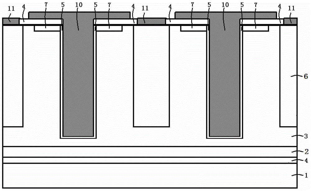
[0042] Figure 6 It is a schematic cross-sectional view of a horizontal structure trench Schottky semiconductor device of the present invention, combined below Figure 6 The semiconductor device of the present invention will be described in detail.

[0043] A trench Schottky semiconductor device with a horizontal structure, comprising: a substrate layer 1, which is an N conductivity type semiconductor silicon material, and the doping concentration of phosphorus atoms is 1E19 / CM 3 ; The insulating layer 4 is silicon dioxide, located on the surface of the substrate layer 1; the inversion layer 2, located on the insulating layer 4, is a P conductivity type semiconductor gallium nitride material, and the doping concentration of magnesium atoms is 1E18 / CM 3 , with a thickness of 0.2um aluminum nitride buffer layer and 2um P conductivity type semiconductor gallium nitride layer; drift layer 3, located on the inversion layer 2, is N conductivity type silicon doped semiconductor gall...


PUM


Abstract

The invention discloses a grooved Schottky semiconductor device with a horizontal structure. The grooved Schottky semiconductor device has the advantages that the semiconductor device is large in conduction area as compared with the traditional Schottky diode with a horizontal plane, and accordingly is high in current density; the semiconductor device is provided with an inversion layer or second conducting semiconductor materials on the surface of the device, and charge can be compensated for the inversion layer or the second conducting semiconductor materials and a drifting layer, so that a reverse blocking characteristic of the edge of the device can be improved. The invention further provides a method for manufacturing the grooved Schottky semiconductor device with the horizontal structure.

Description

technical field [0001] The invention relates to a Schottky semiconductor device with a horizontal structure trench, and also relates to a preparation method of the Schottky semiconductor device with a horizontal structure trench. The semiconductor device of the present invention is a basic structure for manufacturing power rectifying devices. Background technique [0002] Power semiconductor devices are widely used in power management and power applications, especially semiconductor devices involving Schottky junctions have become an important trend in device development. Schottky devices have the advantages of low forward turn-on voltage and fast turn-on and turn-off speed. At the same time, Schottky devices also have disadvantages such as large reverse leakage current and cannot be used in high-voltage environments. [0003] Schottky diodes can be manufactured through a variety of different layout techniques, the most commonly used is the vertical conductive structure of ...

Claims


Application Information

Patent Timeline
Patent Type & Authority Patents(China)
IPC IPC(8): H01L29/872H01L29/417H01L21/329
CPCH01L29/417H01L29/66143H01L29/872
Inventor 朱江
Owner 北海惠科半导体科技有限公司
Why Eureka
Try Eureka