
PCB hole site and hole diameter detecting system and detecting method

A detection system and hole position technology, applied in the direction of measuring devices, instruments, optical devices, etc., can solve the problems of multi-working hours, labor energy, enterprise economic loss, impact on delivery time, etc., to save human resources and reasonable structural design , the effect of fast detection speed

Inactive Publication Date: 2014-02-05
CHENGDU JINDALI TECH
View PDF7 Cites 22 Cited by
  • Summary
  • Abstract
  • Description
  • Claims
  • Application Information

AI Technical Summary

Problems solved by technology

[0002] With the development of electronic industry technology, the market has higher and higher requirements for the drilling quality of PCB boards. However, due to the limitation of testing equipment, it is impossible to comprehensively test the hole position accuracy of printed boards processed by drilling machines. Sampling inspection can be adopted, even if it is sampling inspection, it is manually positioned and inspected one by one, which will cost a lot of working time and energy of workers, so it is inevitable that some parts with unqualified drilling will enter the next process. It will cause waste of materials and time, and in severe cases, it will also affect the delivery time, which will cause greater economic losses and reputation losses to the enterprise

Method used


Image

  • PCB hole site and hole diameter detecting system and detecting method
  • PCB hole site and hole diameter detecting system and detecting method

Examples


Embodiment 1

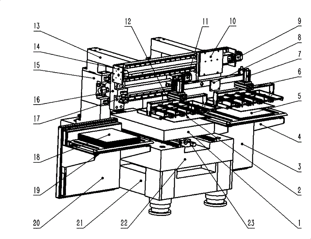
[0038] Such as figure 1 As shown, the driving part 3 of the feeding worktable consisting of a motor, a lead screw and a lead screw nut drives the feeding workbench 4 to rise by one plate thickness unit, and the upper and lower cylinders 7 of the manipulator move downward. When the right manipulator 6 grabs the undetected After the PCB board 5 and the left manipulator 12 grab the PCB board 2 that has just been detected, the upper and lower cylinders 7 of the manipulator rise, and then the left manipulator 12 and the right manipulator 6 are driven by the manipulator drive part 9 composed of a motor, a lead screw and a nut. Driven to move to the left as a whole. When the left manipulator 12 grabs the newly detected PCB board 2 and moves to the top of the unloading workbench 19 and the right manipulator 6 grabs the undetected PCB board 5 and moves to the top of the detection workbench 1, the upper and lower cylinders 7 of the manipulator move downward. , the left manipulator 12 p...

Embodiment 2

[0041] The difference between embodiment 2 and embodiment 1 is that there is an unloading workbench 19 at the bottom of the same side of the camera support beam 15, which automatically unloads the detected PCB, saves labor and improves detection efficiency.

[0042] The manipulator driving part 9 is a screw transmission mechanism composed of a motor, a leading screw and a leading screw nut


PUM


Abstract

The invention discloses a PCB hole site and hole diameter detecting system and detecting method which solve the problems that at present, comprehensive detection of the indexes like hole sites of a printed board completed through a drilling machine can not be achieved due to the limitation of testing equipment, and the detecting efficiency is low. The PCB hole site and hole diameter detecting system comprises a feeding device. The feeding device comprises a feeding workbench drive part. The feeding workbench drive part is provided with a feeding workbench. A mechanical arm supporting beam is connected with a mechanical arm supporting beam connecting frame, the mechanical arm supporting beam connecting frame is fixedly connected with a mechanical arm connecting frame, and a left mechanical arm and a right mechanical arm are fixed on the mechanical arm connecting frame. The mechanical arm supporting beam is further provided with a video camera supporting beam, the video camera supporting beam is fixedly connected with a video camera mounting plate, and the video camera mounting plate is provided with a detection video camera. A main control computer is used for comparing the element of an image captured by the detection video camera and a designed standard value, hence, a PCB is detected, and whether the PCB is qualified or not is judged.

Description

technical field [0001] The invention relates to a PCB detection system and detection method, in particular to a PCB hole position and aperture detection system and detection method. Background technique [0002] With the development of electronic industry technology, the market has higher and higher requirements for the drilling quality of PCB boards. However, due to the limitation of testing equipment, it is impossible to comprehensively test the hole position accuracy of printed boards processed by drilling machines. Sampling inspection can be adopted, even if it is sampling inspection, it is manually positioned and inspected one by one, which will cost a lot of working time and energy of workers, so it is inevitable that some parts with unqualified drilling will enter the next process. It will cause waste of materials and time, and in severe cases, it will also affect the delivery time, which will cause greater economic losses and reputation losses to the enterprise. Co...

Claims


Application Information

Patent Timeline
IPC IPC(8): G01B11/00G01B11/12
Inventor 马飞达杨刚
Owner CHENGDU JINDALI TECH
Features
  • Generate Ideas
  • Intellectual Property
  • Life Sciences
  • Materials
  • Tech Scout
  • Unparalleled Data Quality
  • Higher Quality Content
  • 60% Fewer Hallucinations
Learn More